Anyone,
Is there a certain voltage that is considered "optimal" for the the LS/K170 & J74 when figuring out the resistors (R26/28) as per the BOM equation? I have seen anywhere from 10-16 volts applied in the equation to figure out the resistors. The way I think of this is you want enough to saturate but about mid-way between that and the the device break down voltage (using the J74 as the minimum). Is this accurate?
Well, if you have some high idss jfets you are using, you may consider the max dissipation you want them to see and choose a lower voltage. The B1 only runs at 10 to 11 volts at idss, so that is probably the lowest voltage.
Rush
Folks:
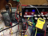
I've reassembled my F5T V3 and the problems I've been experiencing have not been resolved. The attached photo shows the VDC readings: the green meter on the left is connected to the two P output boards and reads 2.1mv and the green meter on the right is connected to the two N output boards and reads 0.0mv. These two meters do not change when I adjust P1 and P2. This is the same result I was getting before I removed the two sets of output boards from the circuit (leaving just the power supply and gain stage board) yesterday.
The yellow meter is connected to the output and ground and reads 2.07 VDC. It also does not vary when P1 or P2 is adjusted.
Your thoughts?
Regards,
Scott
Attachments
Folks:
I've reassembled my F5T V3 and the problems I've been experiencing have not been resolved. The attached photo shows the VDC readings: the green meter on the left is connected to the two P output boards and reads 2.1mv and the green meter on the right is connected to the two N output boards and reads 0.0mv. These two meters do not change when I adjust P1 and P2. This is the same result I was getting before I removed the two sets of output boards from the circuit (leaving just the power supply and gain stage board) yesterday.
The yellow meter is connected to the output and ground and reads 2.07 VDC. It also does not vary when P1 or P2 is adjusted.
Your thoughts?
Regards,
Scott
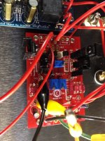
Have you checked if those aluminium bars that are holding the mosfets are not touching a leg of one of them? They seem to be pretty close to the legs on the picture. Even the big washer holding a diode that looks blue on the picture seems to be very close to the legs.
Last edited:
petefrontiers:
You're right, the aluminum angle is close to the MOSFET and diode legs. But they do not touch, and since the aluminum angle is grounded to the chassis I trust the circuit or amp fuse would blow if they came into contact.
Regards,
Scott
Do the multimeter probes are touching the heatsink? I don't like the way you put them on the picture.
petefrontiers:
I put the probes on the heatsinks just to get them in the photo; the readings were the same when the were hanging to the sides or lying on my workbench. I also tested the three meters to make sure they were consistent with each other, and they are.
Regards,
Scott
I put the probes on the heatsinks just to get them in the photo; the readings were the same when the were hanging to the sides or lying on my workbench. I also tested the three meters to make sure they were consistent with each other, and they are.
Regards,
Scott
petefrontiers:
I put the probes on the heatsinks just to get them in the photo; the readings were the same when the were hanging to the sides or lying on my workbench. I also tested the three meters to make sure they were consistent with each other, and they are.
Regards,
Scott
Ok, it looks like your voltage is drained to the ground from somewhere so I'm trying to remove each option. Do not rely only on the fuse, check for continuity between each legs of diodes and mosfets and even the thermistors to the heatsinks.
petefrontiers, SirByrd and Buzz:
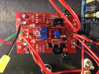
You guys are clearly on the right track. I have replaced the homemade spreader bars from the MOSFETs and installed washers instead. I'm getting some inconsistent readings between the N and P sides of this amp. With one probe connected to the chassis ground, I'm getting the following readings:
With the PS attached to the N and P output boards and the gain stage board
All N output board MOSFET gate, drain and source legs show low resistance, which slowly increases
All N output board diode legs show low resistance, which slowly increases
All P output board MOSFET drain legs show low resistance, which slowly increases. The gate and source legs show as open circuit
All P output board diode legs show as open circuit
With the PS detached from the N and P output boards and the gain stage board
Open circuit for all N output board MOSFET gate, drain and source legs
Open circuit for all N output board diode legs
Open circuit for all P output board MOSFET gate, drain and source legs
Open circuit for all P output board diode legs
To be clear, I understand the leg orientation on the MOSFETs to be, reading left to right with the printed side of the device facing up and above the legs: G D S
The minimum resistance across R5 (using TP3 and TP4) is 823R. Rotating P1's screw increases resistance slightly (about 1R per complete rotation of the screw)
The minimum resistance across R6 (using TP1 and TP2) is 0R. Rotating P2's screw increases the resistance
Even I can see something's up. Your thoughts?
Regards,
Scott
Attachments
First things first. With multi-meter set to measure resistance, attach common probe to the heatsink and the remaining probe to the drain of each mosfet. Every fet should read as an open circuit or infinite resistance. If not, you do not have proper isolation. Start there.
BTW, it should not matter if you have the PSU attached ot not.
BTW, it should not matter if you have the PSU attached ot not.
Folks:
With the power supply detached from the output boards and gain stage board, I get infinite resistance between the chassis and the drains on each of the MOSFETS.
However, when the negative and ground power supply leads and N gate and output connections are connected to the N output boards, I get readings (which slowly increase) between the chassis ground and the drains on each of the N MOSFETS. The same holds true for the P side.
I disconnected the output and gate connections between the N output boards and the gain stage board and the power supply connections to the N output boards and, not surprisingly, again got infinite resistance between the chassis and the drains on the N MOSFETS. However, if the negative and ground power supply leads were reconnected to the N out put boards (but the gate and output remain disconnected from the gain stage board), the resistance between the chassis and N MOSFET drains was about 12.8M.
The pinouts on the 2SC4793 and 2SA1837 seem consistent across all manufacturers. The same seems true of the 2sk170 and 2sj174. They are all properly oriented. My resistors are in the right places; I've got 5.6k at R27/R28 and 12k at R25/R26, but otherwise everything is in the right place with no obvious flying leads, bad solder joints and the like.
Recommendations?
Thanks,
Scott
Attachments
petefrontiers, SirByrd and Buzz:
You guys are clearly on the right track. I have replaced the homemade spreader bars from the MOSFETs and installed washers instead. I'm getting some inconsistent readings between the N and P sides of this amp. With one probe connected to the chassis ground, I'm getting the following readings:
With the PS attached to the N and P output boards and the gain stage board
All N output board MOSFET gate, drain and source legs show low resistance, which slowly increases
All N output board diode legs show low resistance, which slowly increases
All P output board MOSFET drain legs show low resistance, which slowly increases. The gate and source legs show as open circuit
All P output board diode legs show as open circuit
With the PS detached from the N and P output boards and the gain stage board
Open circuit for all N output board MOSFET gate, drain and source legs
Open circuit for all N output board diode legs
Open circuit for all P output board MOSFET gate, drain and source legs
Open circuit for all P output board diode legs
To be clear, I understand the leg orientation on the MOSFETs to be, reading left to right with the printed side of the device facing up and above the legs: G D S
The minimum resistance across R5 (using TP3 and TP4) is 823R. Rotating P1's screw increases resistance slightly (about 1R per complete rotation of the screw)
The minimum resistance across R6 (using TP1 and TP2) is 0R. Rotating P2's screw increases the resistance
Even I can see something's up. Your thoughts?
Regards,
Scott
Replace pot on R5 side. Test pot adjustability again after doing so.
Hi all!
Is the F5T circuit limited in terms of rails voltage by R3 (10), R7/R8 (220/220) and their symmetricals, since they form a voltage divider between output and gnd? I've done some calcs here as if the amp were ideal and driving a sine wave, and for not exceeding their rated max dissipation, rails voltage shouldn't exceed +/- 40V.
Since I'd like to use this amp with an existing PSU of +/- 60V (with less bias and more dissipation, of course), is there any way to circumvent this issue? Perhaps also changing R3?
Thank you for the attention
Daniel
- Home
- Amplifiers
- Pass Labs
- F5 Turbo Builders Thread