the resistor heat is not a problem. for low watt resistors you can use 0.6w if you like.
and source resistors is dual 3w or dual 5w if you like.
my F5 pushing 0.85A bias pr divice at 24.4V with singel 3w resistor, and they dont realy get hot. but som spacing up fom the PCB is recommended.
and source resistors is dual 3w or dual 5w if you like.
my F5 pushing 0.85A bias pr divice at 24.4V with singel 3w resistor, and they dont realy get hot. but som spacing up fom the PCB is recommended.
Risking condemnation and being tarr'd and feathered, run out of town.
Nah, no problem. Everybody has a right to their opinion, and in any case, I find the debate interesting and stimulating.
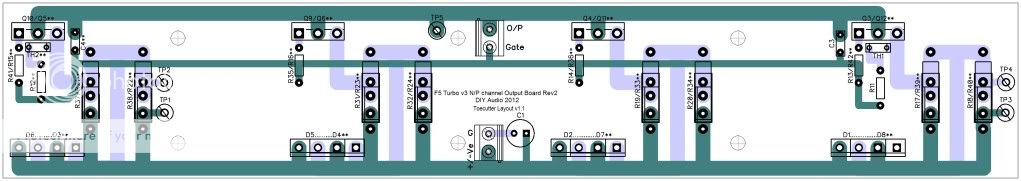
On the V3 type output boards, why are the power resistors "buried" inline with the mosfets? It seems to me that they should be slid out from that line, both for heat reasons and for heat reasons. Both of those reasons, and also by doing so larger resistors can be accommodated than the minimum size. Those resistors that use the flatpak plastic case (Vishay/Caddock) also require heatsinking, I'd have left ample space for that possibility, and used the maximum width of the board possible for larger format resistors.
The power resistors connect to both the MOSFETs and the diode arrays. I guess it's just more convenient to put them there. Bear in mind that the MOSFETs and the diode arrays are actually 'off board'. It's only the legs on the PCB.
TO-220 pack resistors are catered for. You don't have to mount them facing the same way giving you enough room to fix them to a small heatsink.
On the V2 combo board, neat layout to the eye is nice, but as I was trying to convey early on, good looking and good performing are not always the same. Asymmetry is not something that needs to be avoided all the time. Here too, I have concerns about the resistor placement and layout for the larger ones. Also the pad size as I mentioned early on. Better to push the limits in size.
The minimum resistor pad size is 2.5mm as requested earlier in this thread.
The larger resistors, yes they are perhaps close together but the silkscreen of the resistor is oversized so should be OK.
I like symmetry :-(
On both the V3 output board and the V2 board there is much dead space. PCB mfrs charge by the the area, not the layout... so I'd try to spread out the component layout, both from a heat point of view (these are GOING to run HOT) and the ease of service and construction point of view. On the V2 board I see some small resistors sandwiched tightly because the position of a header, C3 means that R11 is right there... sure, it will fit, but why so tight? (just one obvious easy to see example...)
Yes, plenty of dead space, I agree. However, the dead space is there because the MOSFETs need good spacing.
The prototype run is to determine where there are problems. I don't have too many concerns in regards to the 'front end' components being a close fit as there is not too much dissipation to worry about. Bear in mind that Papa specifys 1/4 W resistors and I have allowed for 0.6W.
The TPs position assumes that the final installation will provide easy access to the TPs from the "top" of the board. Not a good assumption. Probably they will not be accessible at all from the top, rather one will have to fish in from the top of the amp, which works out to be the side of the board. So, having them inline makes it easy to short them out with a meter probe. I'd have set them at what would be 45 degree angles looking down on the board, and added space from the Pots - the pots could be top or side adjust, which makes it easy enough for the screwdriver to slip off if side adjust again shorting the TPs (unless the TPs are socket type in which case you can't get to them from the side, so assume uninsulated pins) - the step spacing making it possible to get to the TPs from various angles.
I'll concede on the test points. The specified ones have a 'loop' sitting on an insulator so should be OK. I'll await some feedback from the prototype builders.
Since these boards are going to be slapped on MAJOR LARGE heatsinks, usually standing vertically from the main chassis, there is not a whole lot of benefit from making the tightest layout using the smallest board possible. In fact there are deficits in terms of layout options and heat build up.
I don't think I've done that.
The converse view is that there's no point in making the boards so long that every builder has to choose an incredibly deep chassis.
Bear in mind that builders can choose the single output boards and mount them wherever they want. I certainly didn't intend that people would use the V3 output board (4N or 4P MOSFETs) and bias so high. If people want a 'beast' they can use two output boards per rail and spread them over a deeper heatsink
Making the boards have a larger long dimension, as long as it does not effect stability, is a BIG advantage because you need space to permit each mosfet to adequately flow heat to a region of the heatsink.
See my response above
Folks who are using front to back heatsinks on a deep chassis, and using this sort of board are really only getting part of the heatsink value that they have paid for, because the heat is being generated only in the central portion. Yes the rest of the heatsink helps, especially once it has been cooking for a while, compared to a shorter extrusion, but it is none-the-less not as effective as wider spacing. So what's the loss in adding a few inches in length to this sort of layout if it buys better heat transfer and wider component spacing with fatter traces and bigger pads??
I don't know how much wider I could go.
I was asked if I could get the board to fit a 300mm deep chassis, and I laid out to that. If somebody wants to use a 500mm chassis they can have two next to each other, if the want to use a 400mm chassis they can use the single output boards.
Looking cool and sexy by being compact and packed in, is a false design goal or aesthetic, imo.
One should de-rate ALL the components based on heat rise over 70F (whatever that is in C) ambient temperature. In summer conditions the environment around that board is going to get VERY HOT, reducing the effective wattage of all of the resistors. Me, I want max space and max air flow.
Count on designing from an ambient air temp of >100F (whatever that is in C?), add in the temp rise due to the circuit, and then you'll see why this is important.
Personally, I do not what to listen to a great amp and fans. Not if it is possible to NOT listen to fans. If it is a fan, the slower the fan, the higher the VOLUME and the lower the velocity of air, the better... but would rather not hear or have a fan full time.
If ur building right now - do NOT put ur small resistors flat to the board!! Make sure you put about 1-2mm or ~0.64" or so minimum clearance between the resistors and the board. More is better. Less clearance is worse.
I'd want more spacing resistor to resistor for the "small" wattage ones, again for heat purposes. If I had to build on these boards, I'd end up putting every other resistor high (a full extra resistor body diameter) off the board on it's leads to permit adequate air flow, not in-line at the same height. High - low - high - low - high - low ...etc.
My only other thought at the moment is "black"?? What sort of material is it? Black is usually a carbon based pigment which is not a particularly good insulator, albeit probably up in the MOhms, but still of some concern... also black will absorb heat from outside sources better... and there is heat to be absorbed being next to the heatsinks....
It's a standard PCB solder mask pigment. What else can I say?
All of this may be nit picking, but maybe not given the heat that this amp will put out. Optimizing for heat may be important.
Oh, speaking of which, a good way to test heat is to pick up a cheapo non-contact thermometer. Great stuff for testing temps on electronics!
Please don't stone me?
_-_-bear
PS. Toecutter, I think you've done a great effort, please make sure that this message comes across...
Bear
I take all of this on board.
I'm not about to get too precious about it.
I can't say I agree with everything you say (although I do agree with some of it) however the prototype builds will hopefully answer alot of the questions and lay the foundation for a second board batch.
I hope I've not come across as over defensive. I really do value the input that you and all the other forum members have contributed to the board layouts. Long may it continue....
PPS... someone mentioned copper being bright finished as not a good radiator of heat? Not sure about that at all, but if that is an issue there are a variety of chemical agents that can put a thin black finish on copper... of course of those agents create an insulative layer, maybe not so good... heh. Something to look into.
Yess I did
Simple principle white radiate less than black.
Anodise Alu sink and eficency increase.
Cooper is like miror like so does not radiate to well
But put a fan there and eficency goes up as Copper conduct heath beter than Alu and sink size goes way down
That is way is used on CPU coolers those litle babies are designed to dissipate over 100 W of heat if one is willing to put up with the noise.
Also cooper easy to solder/ braze just get thick plate and shitload of thin fins one can make its own sinks (if one can aford the cost)
Alu can be welded if one got the equipment and skill but what the point as extruded stuff can be had
Painting cooper I pass I am dangerous when any where near a paint brush.
Maybe you willing to try?
Bear,
How about this one.....?
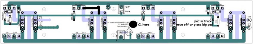
MOSFET spacing is 80mm. Resistors moved about a bit.
Size of board is 290mm x 50mm.
Mo bettah.
You might want to run the trace that goes from the Mosfet leg to the resistors horizontally rather than down and back up... that way you can add some pads and holes at an even wider spacing.
I know people say that these resistors won't get hot, but based on the F5 I have worked with, fully biased they get hot, and if this Turbo is fully biased up for low Z loads, I expect it will pass a fair amount of juice...
Also that C1 cap would do well to move up and over, and the TP on top can be moved to more open space too... and of course the dual TPs are not offset here...
If it were up to me I'd do much the same on the V2 board...
I get what you are saying about the single board outputs...
I was more talking about using the space between the mosfets on the existing board layouts rather than making a new board that has more distance between mosfets. What are we calling that, length? width? Ok the "long dimension."
The black coating? dunno. usually I see clear and green...
_-_-bear
Bear, I created the 80mm spacing layout some time ago to try and match the UMS. It doesn't match the UMS actually anyway but I had it on my PC already so I tweaked it a bit with your suggestions.
UKtoecutter, I tried to show what I am talking about with a crude markup...
TP5 should also be moved to another area, so that it no longer is in line with what is now below it... maybe over to the right between another pair of mosfets...
_-_-bear
TP5 should also be moved to another area, so that it no longer is in line with what is now below it... maybe over to the right between another pair of mosfets...
_-_-bear
Attachments
Last edited:
and also. C1 need to be turned 180degree on P channel?
same on the original output board. C1 and C2 need to be changed a bit. they must be monted the same way.
and turned 180 degree on P channel.
EDIT: never mind") just use C1 on P channel and C2 on N channel
just use C1 on P channel and C2 on N channel
same on the original output board. C1 and C2 need to be changed a bit. they must be monted the same way.
and turned 180 degree on P channel.
EDIT: never mind
just use C1 on P channel and C2 on N channel
Last edited:
I had offered more than 500 free blank JLH PCB on this forum. As I mentioned before this is another free PCB project. Several members PM me to push it forward. If this is not allowed I will make only 2pcs for my personal project.
I am not sure what the law or policy is.
But SiliconRay is a commercial entity, and taking NP's designs and using them commercially probably is not proper.
I know other designs are "used" by third party commercial entities and sold elsewhere, but not by participants in this forum, AFAIK.
Perhaps a moderator or NP should comment??
Regards,
_-_-bear
and also. C1 need to be turned 180degree on P channel?
same on the original output board. C1 and C2 need to be changed a bit. they must be monted the same way.
and turned 180 degree on P channel.
EDIT: never mind
Yes, quite right about C1...
I'll ammend.
- Status
- This old topic is closed. If you want to reopen this topic, contact a moderator using the "Report Post" button.
- Home
- Amplifiers
- Pass Labs
- F5 Turbo Circuit Boards