You should start another thread for this guy, as it has more aspects than a cat has hair. I've been thinking of doing a push-pull for quite some time myself, and there are many ideas from the tube world that could be adapted. I'm also awash in tube iron now, so I could throw a couple of pieces at a project like this. I'll probably wait until I flush all my single-ended projects through the system. The amp in my "Das Ist Aber Schade" thread hasn't even been powered up....
Last edited:
You should start another thread for this guy, as it has more aspects than a cat has hair. I've been thinking of doing a push-pull for quite some time myself, and there are many ideas from the tube world that could be adapted. I'm also awash in tube iron now, so I could throw a couple of pieces at a project like this. I'll probably wait until I flush all my single-ended projects through the system. The amp in my "Das Ist Aber Schade" thread hasn't even been powered up....
Hi wrenchone,
thats a good idea, in no way I meant to hijack your thread here... actually I like what you are doing and even quoted you in the article ;-)
Just wanted to add my experiences with the Semisouth JFETs...
By the way, the iron I used for the P-P output transformers are regular power supply toroids (2x 115V / 2x 12V / 240VA) , little cost but great results
will look for that other thread, the name is great!
I wan't really peeved, but your effort is sufficiciently different that it deserves a thread of it's own. I think it's neat that people are finally getting around to dropping silicon (and more exotic materials) into traditional tube circuits. The "Das Ist Aber Schade" effort could be morphed into a push-pull topology without too much extra effort. I'll save more extensive comments for the new thread...
I would really love to see your schematic.Attached is a photo of the first proto of an SE amplifier( the "SiC Puppy") using the Semisouth 085 silicon carbide JFET in the output stage. The front end uses the Supertex DN2540N5 depletion mode mosfet. I choose the Semisouth part over the IXYS depletion mode parts due to the extra headroom afforded by the 1200V rating, allowing me to choose B+ voltages with a bit more freedom. The circuit (to follow) is set up just as if the two parts were pentodes, with partial feedback from the output drain to the input drain, plus a limited amount of global feedback (disconnected at firtst. I used the One Electron UBT-1 1.6k transformer because I had a pair on hand. The output stage bias is set for the maximum primary current rating of the UBT-1 (150 ma). Next is a power-up with a DC supply to chcek stability of the output bias.
The heat sink is one of Papa Zen's giveaways from the very first Burning Amp in October 2007. I'm thinking of running the amp in a dual mono configuration using a pair of ~150VA step-up/isolation tansformers, which when configured for 230V output and rectified will give me ~320VDC B+. There is an on-board capacitance multiplier for ripple reduction, feeding a 270uF bulk capacitor.
More to come - this is just the first heads-up.
I threw the SiC Puppy on the HP4194A gain-phase analyzer this afternoon, and got squirreley behavior near and beyond gain crossover, no doubt due to the output transformer. To add extra sauce, the scans for each channel were different, possibly due to changes in output transformers, even though they are the same vendor/part number (very different revs, obviously). Some extra compensation and a damping network will be needed so that things line up with my expectations. I'll document when I get results that satisfy me.
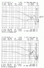
I added some compensation around the feedback resistors of the Sic Puppy and got the resulting gain-phase plots. Each plot shows one channel of the amplifier. The top plot shows the "good" channel, with a resonance appearing at somewhere between 3-4 MHz. The second "bad" channel shows a resonance occurring at ~500 kHz, and a second one in the same place as the good channel. In both plots, the gain crosses 0 dB, then pops up above zero at higher frequency. This is an indication of possible trouble with a difficult load (like a speaker, for example), and is something that needs to be fixed.
Attachments
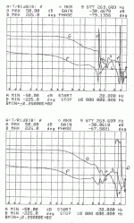
This next set of plots shows the gain and phase with a 20 ohm + 33 nF Zobel network placed agross the output. The bottom plot shows the good channel. The Zobel has pushed the high frequency gain down such that it always stays below 0 dB after gain crossover. That's a good thing.
The top plot shows the bad channel. The Zobel in this case also keeps the gain below 0 dB after crossover, but the gain crossover frequency is defined by the first resonance, which is a problem. I was blaming this extra resonance on the output transformer, but there may also be a problem in that channel that I don't understand. Switching the transformers would be an easy way to ascertain that, and I may try it tonight.
The top plot shows the bad channel. The Zobel in this case also keeps the gain below 0 dB after crossover, but the gain crossover frequency is defined by the first resonance, which is a problem. I was blaming this extra resonance on the output transformer, but there may also be a problem in that channel that I don't understand. Switching the transformers would be an easy way to ascertain that, and I may try it tonight.
Attachments
I managed to swap the output transformers, and the gain-phase problem follows the iffy transformer. The solution for the time being will be to steal a UBT-1 from one of my other projects, bodge it in, and see if it fixes the issue. I already have yet another pair of UBT-1s coming courtesy of Fleabay (2 for the price of one!).
Sisyphus comes to mind.... I tested the channel with the replaced transformer on the gain-phase analyzer. The initial plot looked good, then that channel promptly promptly broke. Hopefully I can fix this (and have it stay fixed) in time for BA. It's an opportunity to re-center the bias on both channels and do some other maintentence things.
OK, this thread revives after a long dormancy. I was too lazy to leap right on some of the original design issues back in 2013, because the original "SiC Puppy" circuit sounded quite nice as it was, but I'm now going to present a couple of more modern (hopefully improved) variants of the original design.
One variant will either use some of the original Semisouth 085 SiC jfets I still have on hand (my boss gave me 2 tubes of them to play with way back when), or the United Silicon Carbide version of the part that is quite similar, currently available for a reasonable price, and may have better/tighter gate leakage characteristics, since USC has after all had 10 years to step up their game and improve their process. The new circuit will incorporate a follower to drive the leaky gate and the lowish value gate pull-down resistor necessary to keep the SiC jfet bias from running away. This will allow me to put a much more modest coupling cap and higher value pull-down resistor ahead of the follower.
I'm also going to present a second circuit that will use a SiC enhancement mode mosfet at the output (there are many to choose from these days, but I'll go for a 1200V device for safety margin). The mosfet will use a bias circuit to wake it up and set an appropriate output DC bias current. I may also incorporate the same follower gate driver as in the jfet version to make sure that gate capacitance doesn't pose a significant lag to the control loop.
Both circuits will use "Schade" feedback as originally employed in the "SiC Puppy" design, so that the output device (whichever flavor) emulates a triode. I'll also be using some global feedback to tighten up the output XFMR response, especially in the bass. The original circuit used the One Electron UBT-1 output transformer, but in the newer design, I may opt instead for the UBT-3, which with a 3k primary impedance has a more extreme step-down ratio than the UBT-1 and may allow me to use a lower DC bias current for the output stage.
In the original "SiC Puppy" design, the 150 mA output bias current posed a significant challenge for thermal design, as the die in the Semisouth 085 jfet was on the small side, with only a modest junction - to - case thermal impedance. I used heat spreader plates cooled by a microprocessor heat sink/fan combo, so the heat got adequately removed. I'd like a design that didn't blow so much power in the output stage.
I originally used the Supertex (now Microchip) DN2540N5 depletion mode mosfet as the input device, which is what was available at the time. It sounded OK, but has too much input capacitance for my taste these days. I'll be replacing it with the smallest IXYS/Littelfuse 1000V TO-220 depletion mode device with a much lower gate capacitance. Since I don't like to court fate these days, I'll also be incorporating an input gate protection clamp circuit that is biased up to present a low capacitance at the amp input.
All in all, the basic thrust of the design hasn't changed, that being to emulate a classic 2-stage Class A single - ended vacuum tube amplifier with Schade feedback using modern semiconductors instead. When I get to work tomorrow, I'll upload the two circuits for inspection. There are currently a lot of "TBDs" for the component values, which should get sorted out as the designs proceed.
I also nabbed a couple of nifty toroidal isolation/step-up transformers from now-defunct Halted, which should work well to provide the B+ for the design without spraying stray flux all over the place and causing hum problems, something that put a significant crimp in the original design. The first design cut used an isolation/step - up transformer wound on a split bobbin - excellent for isolation, but it sprayed flux like a tom cat with leaky kidneys and caused significant hum problems until I replaced it with a potted transformer in a shielded metal case.
More later,
Wrenchone
Last edited:


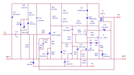
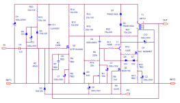
Here are the two design structures I'm contemplating - some values are still TBD, as I will need to characterize the new devices I'm using for input and output. The input devices should be IXTP01N100D. These have only 100 pF gate capacitance, as opposed to the 300-odd pF gate capacitance of the DN2540N5s I originally used at the input. Un fortunately, the IXYS devices appear to be in short supply, but I think I have enough left in my stash to get things going.
Attachments
Last edited:
I also have the option for using the smallest 500V depletion mode device that IXYS has to offer for the input stage - the supply in stock looks to be better for those devices, and since it's at the input rather than driving the output transformer, there's a generous amount of voltage margin.
Since I've already ordered mine, I guess I can tell you - it's the Ixys/Littelfuse IXTP02N50D. The input capacitance is around 120 pF, much smaller than that of the DN2540N5 I originally used at the input of the first version of the "Sic Puppy" amplifier. At 500V vs. 400V, there's more voltage margin, too.
Last edited:
- Home
- Amplifiers
- Pass Labs
- "SiC Puppy SE Amp Using Semisouth 085 JFET