Next thing to look out for - resistors with overly optimistic wattage ratings.
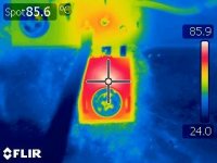
Everyone wants things to be smaller and cheaper. With resistors, this can be counterproductive. I have on hand 3W resistors that are not much bigger than a 1/2 W part, and really should be rated at 3/4-1W. The smaller resistors just get hotter for the same dissipation. This may not hurt the resistor much, but it can be pure hell for adjacent components and the PCB. What started this rant were "2W" resistors derated by 50% that were still cooking at 130-150C (a thermal imager shows up a lot of sins). To make a long story short, several resistors are now physically much larger, and spaced away from critical components (mostly capacitors). I may post some thermal camera images to illustrate my point. The problem children are R3,4,10 and 11. I'm waiting for Mouser to deliver some aluminum oxide TO-247 insulators, which will help the thermal interface between the heat sink and the Semisouth FET, as will as improving HV isolation.
Everyone wants things to be smaller and cheaper. With resistors, this can be counterproductive. I have on hand 3W resistors that are not much bigger than a 1/2 W part, and really should be rated at 3/4-1W. The smaller resistors just get hotter for the same dissipation. This may not hurt the resistor much, but it can be pure hell for adjacent components and the PCB. What started this rant were "2W" resistors derated by 50% that were still cooking at 130-150C (a thermal imager shows up a lot of sins). To make a long story short, several resistors are now physically much larger, and spaced away from critical components (mostly capacitors). I may post some thermal camera images to illustrate my point. The problem children are R3,4,10 and 11. I'm waiting for Mouser to deliver some aluminum oxide TO-247 insulators, which will help the thermal interface between the heat sink and the Semisouth FET, as will as improving HV isolation.
This is a common enlightenment  I learned a long time ago 1W on a 2.5W resistor is not going to cut it! I now use a minimum rating of 5X and I'm ussually happier with 10X the quiescent power for a "hot" Resistor. I do use alot of 5W, 10W, 12W, 25W and 50W Rs. The thermal distortion or at least the Tc is much lower typically also.
I learned a long time ago 1W on a 2.5W resistor is not going to cut it! I now use a minimum rating of 5X and I'm ussually happier with 10X the quiescent power for a "hot" Resistor. I do use alot of 5W, 10W, 12W, 25W and 50W Rs. The thermal distortion or at least the Tc is much lower typically also. Given the cheating in power rating that goes on these days, this would be one application where steel leads make sense, limiting the amount of heat conducted to the PCB and solder joint from the hot resistor. I've never understood why some inrush protector manufacturers use copper leads....Others will no doubt quibble on sonic grounds - everything involves compromise. Spacing the resistor off the PCB helps. I used ceramic beads made for that purpose at my last job - can't find a source for them now. Some resistor manufacturers squish the leads or put a jog in them to get the spacing.
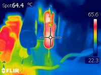
Well, I changed the resistors, and they are not running any higher than 65C now, which is quite a change compared to the 100C+ temperatures on the first revision of this design. Bias current drifts up about 10ma (from 150 ma to 160 ma) as the amp warms up, probably due to change in leakage current. The gate is at ~1.5V with a 10k gate resistor, meaning there is ~150uA of gate leakage. I may incorporate a source follower in the next pass of this design to eat the leakage current. A really ammbitious follower is not needed - I may be able to get by with a pair of 35 cent jfets, at the cost of adding some low voltage rails.
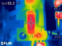
The 085 die temperature is at ~90C after sitting a while. An aluminum oxide washer helps the thermal resistance of the Semisouth part - the heat sink actually starts to get warm now... At any rate, with 302V of drain voltage and 160ma bias current, the power dissipated in the 085 is 48.3W. The die temperature ris is ~65C (25C to 90C), so the total thermal resistance of the interface is 65/48.3 = 1.35 degrees C/Watt.
This is probably good enough for the time being to try driving the amp into a load of some sort - more later.
I would worry about the solder bond to the package and the epoxy at temperatures much above 150C. A more important issue is the stress from thermal cycling, which can delaminate or crack the chip. The 085 has high thermal rresistance as it is.... I wonder how they do the bond-down anyway? I'll ask someone downstairs at work.
Another issue is that pesky gate leakage, which I believe is responsible for the bias current creeping up as the device heats up. I'll monitor the gate voltage next time I have the amp on the bench to see if this really is true.
I'm happy that I appear to be able to get away with blowing 45 watts in a TO-247 without melt-down. The aluminum oxide washer I'm using as an interface helps a lot. They're thick enough so that cracking doesn't appear to be a big problem. I need to now invest in some conical washers and a torque wrench, which will help keep the mounting screws tightened consistently. I'll probably use these in some of my other Class A projects.
I would worry about the solder bond to the package and the epoxy at temperatures much above 150C... I wonder how they do the bond-down anyway?...
175C is a typical "shutdown" temp built into devices of "normal" Silicon. It also can be expected to be 15-20 X accelerated life. (1 day would be the equivalent of 15 or 20 days!). I would expect the package to be the stumbling block.
I've been downstairs a few times
There are several processes and I do not know any SiC process details but: Silicon die are ussually soldered to the package substrate with a silver paste in an oven the reaches 350-450C over the coarse of an hour maybe, depending on the process (450C is very common). Talk about accelerating life! The die bond process must be considered in the big scheme of things. Every process the die goes through may expose it to more heat. Growing further oxide thickness or defusing junctions deeper. Therfore higher temp processes are first and every sucsessive one lower temp. There are lower temp, coductive epoxy die bond processes. The die likely makes at least one direct electrical contact with the pkg substrate. Ussually the Drain of a MOSFET. The Gate and Source can be wire bonded. Bonds are ussually acoustically welded(what a coincidence). Many wires are used on the Source. There are other pakaging configurations but we're thinking TO-247 here. If it is encapsulated the epoxy used becomes soft at some temp ussually about 175. It can move around and it can exert pressure on the wire and wire bonds. There is also bumps, but we'll save that for another time.
I'm quite familiar with the bonding processes for typical Si parts. A lot of the time conductive epoxy is used. Some use solder - I used to see that a lot on TO-3 parts. I don't know what they use for SiC. I gave one of the process/packaging guys downstairs from me an 085 to play with. I never heard anything back from him - time to corner the bloke and make him cough up.
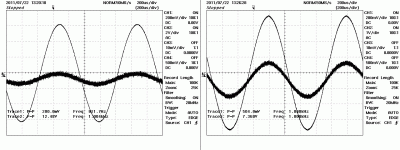
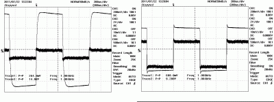
I have one channel working more or less satisfactorily, though somewhat shy of the desired value for output stage bias current (120ma vs 150). I went ahead and loaded the 8 ohm tap of the output transformer with a 10 ohm resistor, and did open loop and closed loop excitation with sine and square waves. The first picture shows result from sine excitation. The left-hand set of waveforms is with partial feedback (R7 is connected, C2/R6 are not). The gain under these conditions is ~62X (36 dB). With the loop closed around the transformer 8 ohm secondary (using R6, with partial feedback resistor R7 still in place - C2 is not stuffed), the gain is 14.6 (23.3 dB).
Attachments
Last edited:
This next set of pictures shows open loop/closed loop square wave excitation. Closing the loop around the transformer tightens up the square wave response. There is output overshoot, but it is just the overshoot of the input waveform amplified. The amplifier looks stable without compensation capacitor C2. The other breadboard I have exhibits low gain and a distorted triangle output with 1kHz square wave excitation. I suspect an accidentally zorched output jfet (ouch!) or a defective output transformer. We'll see tomorrow. When I get both channels satisfactorily operating, I'll push some tunes through them. I'll also do a gain-phase plot of the working channel when time permits.
Attachments
OK, both channels are up, and I ventured powering up a pair of so-so Infinity 2-ways hanging around in the lab, using a fairly venerable Panasonic portable CD player as a source. All the roaring and screaming and fet-fiddling is worth it. Crisp, detailed, lifelike.
I still need to fiddle with the bias current on one of the amps, but the simple tube-derived SE circuit works a treat. Some effort changing around the input fets may be worthwhile, but the Supertex input fets didn't appear to harm the sound any. Obvious one to try would be some of the smaller Ixys depletion mode devices. I may also get better results by pushing more through the input fet and reducing the drain loading resistor, but that experiment will wait until later. This guy will definitely make the trip to Burning Amp.
I still need to fiddle with the bias current on one of the amps, but the simple tube-derived SE circuit works a treat. Some effort changing around the input fets may be worthwhile, but the Supertex input fets didn't appear to harm the sound any. Obvious one to try would be some of the smaller Ixys depletion mode devices. I may also get better results by pushing more through the input fet and reducing the drain loading resistor, but that experiment will wait until later. This guy will definitely make the trip to Burning Amp.
Last week, I powered up both channels of the amp in the lab at work and got a "thumbs up" from the co-workers still hanging around. The amp went home with me to be fitted with a case, fan (throttled down DC fan) and a decent power supply. It was running at work off a nifty Xantrex HV bench supply, a nice piece of kit for a tube fancier with deep pockets, but essential also for folks doing SMPS development.
For the power supply, I plan to try an isolated 115/230V step-up transformer with a full wave bridge, which should give me about 320VDC before my capacitance multiplier. I'm curious to see if one transformer (150VA) will hold up powering both channels - if not, I'll try a dual power supply approach, as I have two of the transformers and paid almost nothing for them. First priority is scrounging around in the basement to see if I can scare up a suitable case.
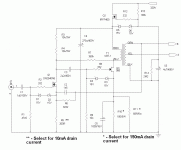
The attached schematic is the one I'm currently using. The values of the parts denoted with asterisks should be changed to get the proper bias current, depending on the parts you have on hand. Leaky 085s (that is, ones with leaky gates) won't work at high drain voltages with a 10k gate resistor, and should be used in low voltage projects - more on that later, as I have far more projects in process than time to work on them.
For the power supply, I plan to try an isolated 115/230V step-up transformer with a full wave bridge, which should give me about 320VDC before my capacitance multiplier. I'm curious to see if one transformer (150VA) will hold up powering both channels - if not, I'll try a dual power supply approach, as I have two of the transformers and paid almost nothing for them. First priority is scrounging around in the basement to see if I can scare up a suitable case.
The attached schematic is the one I'm currently using. The values of the parts denoted with asterisks should be changed to get the proper bias current, depending on the parts you have on hand. Leaky 085s (that is, ones with leaky gates) won't work at high drain voltages with a 10k gate resistor, and should be used in low voltage projects - more on that later, as I have far more projects in process than time to work on them.
Attachments
- Home
- Amplifiers
- Pass Labs
- "SiC Puppy SE Amp Using Semisouth 085 JFET