Gate leakage in a MOSFET is caused by impurities or holes in the Gate Oxide. Between the gate and the channel (Source and Drain) there is an oxide layer grown to a specific thickness. The thickness determines the maximum gate-source voltage. The oxide is a dielectric, no current should flow thru it and it should act like a capacitor to the Source and Drain.
However, they leak? If you don't help the gate stay at the voltage you want it at, the leakage will allow a voltage to develope at the gate. A MOSFET gate left floating will likely float up and turn itself on. A pulldown resistor of some type is always a good idea. It can be very large ussually because there is very little leakage in MOSFETs.
SiC and JFETs??? The level of leakage we are starting to here about in these SiC devices suggests that the pulldown (ussually our input load setting value, maybe 47k) needs to be much smaller or the input leakage will create it's own unexpected bias to the device. Turn it on, off, whatever. If you don't design in for that current to your circuit, you might be suprised. In fact, these currents seem so unussually high, you might need a stronger driver circuit to drive the input resistors to circuits with SiC leakage
Thanks FLG. Is this why Nelson doubled up the 109's on the FE of the J2? Doing so also reduces the resistor size for the bias voltage and lowers source resistance, all adding up to the FE having an easier time driving the SiC devices, correct? More current and less resistance. Also, he talks of a large cap that he has used. Other than for coupling the input, does this help with the gate leakage?
Last edited:
I think the reason N.P. doubled up on the Inputs of the J2 is that the bias voltage needed at the gate of the SiC device is low. Maybe 1.5Vgs vs 4.5Vgs with a MOSFET. This neccesitates a smaller drain resistor from the input circuit or lower current thru the input circuit. This will likely reduce the gain of the input circuit. So, he reduces the drain R of the input circuit to 220 ohm or so and uses two devices to recoupe the lost gain.
I don't know about the large cap? Where?
I don't know about the large cap? Where?
I don't know about the large cap? Where?
The input cap on the amp at the beginning of this thread.
Sorry if this is threadjack, Wrenchone, just trying to understand what you are talking about as I have some of these same parts.
O.K. right. With the smaller Rs at the input, the input cap will be creating a highpass filter. It will have it's f3 raised by smaller Rs unless you use a bigger Cap.
I don't think we're thread jacking, we're talking about his circuit and his discoveries. What we don't know is what we are talking about? Where's the schematic??? Stop trying to be "the one and only" feeding us bread crumbs or something and show us this cupcake?
I don't think we're thread jacking, we're talking about his circuit and his discoveries. What we don't know is what we are talking about? Where's the schematic??? Stop trying to be "the one and only" feeding us bread crumbs or something and show us this cupcake?
The Data Sheet for the R100 SS parts seems to indicate a 0V D-S and a MaxBVds D-S with the Gate at -max G-S and measure gate current. That is: Drain gnd'ed and source Gnd'ed, with the gate at -15V measure gate current. And D@ 1200V and Source Gnd'ed and measure Gate current. (put a large enough resister in the gate line to measure 100uA or whatever)
This is another unreasonable test for us linear operating ClassA nuts? We should put something like 0 to +2.5V on the gate and 2-50V D-S and measure gate current. Like our operating conditions.

Except for Wrenchone: He needs to use 320Vds or whatever and what did he say for the 085 -9Vg-s. Might be more difficult for his SS glass idea with 085?
This is another unreasonable test for us linear operating ClassA nuts? We should put something like 0 to +2.5V on the gate and 2-50V D-S and measure gate current. Like our operating conditions.
Except for Wrenchone: He needs to use 320Vds or whatever and what did he say for the 085 -9Vg-s. Might be more difficult for his SS glass idea with 085?
Last edited:
The reason I doubled up the JFETs on the input of the J2 was not associated
with Gate leakage. In fact, Gate current goes the other way in the
enhancement mode parts since the PN junction is forward biased.
We are talking about Gate current seen in depletion mode, and as I said this
is anywhere from 1 uA to more than 100 uA. If you are biasing the Gate
through a 47K resistor, you will have to allow for that voltage drop. Your
choice (besides going back to Mosfets) is to select for low leakage, lower the
DC source impedance, or provide a tracking mechanism.
This is not unique to the SemiSouth parts - Gate leakage is seen with other
JFET and SIT/Vfet parts.
Select for reasonably low Gate current under the conditions you will use it.
Bias it up, then let it warm up, then bias it again, then burn it in all you
like, then check it again. If the bias wanders due to Gate current after a
few days, then replace it.
Just like a tube!
Bias it up, then let it warm up, then bias it again, then burn it in all you
like, then check it again. If the bias wanders due to Gate current after a
few days, then replace it.
Just like a tube!
If using the R085 in a SE amp like the F3 or ZV3/4, does the leakage vary over the operating ranges of the amp to a degree that you would need to do anyting other than allow for the voltage drop that would occur across the the biasing resistor. Is their any benefit performance wise to a "tracking mechanism". Is Wrenchone experiencing this leakage problem to a greater degree because of the V levels he is operating at or his this something that is determined by the individual devices.
I may have bad parts. The gate reverse voltage goes all the way up to the maximum rating of -15V, but this is still not enough to stabilize the bias. This is at a paltry 225-250V drain voltage, far short of the 1200V maximum rating. I have 10k from gate to ground, and shorting the gate to ground with a clip lead makes no difference.
See! this is why I won't prematurely publish a schematic. Just because you see a board and a heat sink in a picture does not mean things are all hunky-dory and ready to go. I'm going to try tomorrow with a batch of parts I scored thorough Teabag's group buy - maybe they'll behave.
See! this is why I won't prematurely publish a schematic. Just because you see a board and a heat sink in a picture does not mean things are all hunky-dory and ready to go. I'm going to try tomorrow with a batch of parts I scored thorough Teabag's group buy - maybe they'll behave.
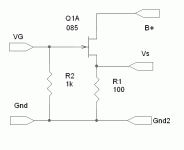
This circuit will be useful to characterize the 085 parts you have. The 100 ohm source resistor should be rated for 5W or better so that it doesn't heat up too much. The 1k Resistor should be right at the gate lead to avoid oscillation.Gate leakage can be determined by measuring the voltage across the 1k resistor. The leakage current will be that voltage divided by 1000. Source current is determined by measuring the voltage across the 100 ohm resistor and dividing the resulting voltage by 100. I use a large CPU cooler with fan to mount the parts in order to have a stable temperature during testing (also so they don't melt/blow up). It's very simple to drill and tap a 6-32 hole in the heat sink to attach the transistor with a screw. Use of a good thermal pad between device and heat sink is a must.
Attachments
Last edited:
This circuit will be useful to characterize the 085 parts you have. The 100 ohm source resistor should be rated for 5W or better so that it doesn't heat up too much. The 1k Resistor should be right at the gate lead to avoid oscillation.Gate leakage can be determined by measuring the voltage across the 1k resistor. The leakage current will be that voltage divided by 1000. Source current is determined by measuring the voltage across the 100 ohm resistor and dividing the resulting voltage by 100. I use a large CPU cooler with fan to mount the parts in order to have a stable temperature during testing (also so they don't melt/blow up). It's very simple to drill and tap a 6-32 hole in the heat sink to attach the transistor with a screw. Use of a good thermal pad between device and heat sink is a must.
Thanks Wrenchone, I have built a pair of AJ monoblocks, but building from a schematic and designing something new are two different things. I am going to try an SRPP with my SS and had not thought of or even considered gate leakage, so this was new to me. Considering that Nelson did not menrion it in the Nemesis article, I am hoping that it is not too big of a problem in typical operating ranges. It seems that your particular attempt is putting it in a worse case scenario.
Well, if this part cannot turn off at a fraction of its rated drain voltage at its maximum rated reverse gate voltage, I'm going to be raising hell in several venues. We''ll see tomorrow. I'm going to use the circuit shown to exercise some of the parts at 300V Vds.
Last edited:
I loaded one of the SS 085 jfets from my Teabag group buy into my test jig, and it preliminarily looks like it should, regulating at ~ 6V negative gate bias for 100ma drain current. Later on when I get a chance, I'll adjust the source resistor for 150 ma drain current and see if the part behaves itself at 300V drain voltage. I'm also using a 1k gate resistor, so I will need to see if the part works with 10k.
This is the first revision schematic for the SiC Puppy. There is nothing at all innovative about the overall architecture, as it is just a simple partial feedback single-ended amplifier with silicon substituted for the customary pentodes. Those looking for background can search out the threads regarding the RH84 and similar amplifiers in the tube forum - there's been lots of discussion. The values shown in the schematic are preliminary, as I have been wrestling with bias issues in the output stage, so I haven't even applied full voltage to the circuit yet, much less a signal.
Issues to look out for:
1) The Semisouth 085 jfet has a relatively small die, as the data sheet lists a junction-to-case thermal resistance of 1.1 degrees/watt maximum. As the design is currently set up for ~45W dissipation in the output stage (I'm trying to wring all the power I can out of this thing), this means that the die can run at 75C at room temperature, even with a perfect heat sink and case to heat sink interface (zero thermal resistance). You'll need a good heat sink and the best thermal interface material you can find to keep the device temperature under control. You can back off on the bias current (and power dissipation) by increasing the values for R10 and R11, at the cost of less output power. The circuit posted previously can be used to evaluate the parts you have and select proper values for the source resistors. I broke up the source resistor into two pieces to spread out the dissipation and avoid hot spots. I'm using 2W metal oxide resistors.
Friday afternoon, I finally found a good 085 and was able to stabilize bias in a test jig at the desired bias current and ~250VDC B+. The values for R10 and R11 in the schematic are from that session, and will not necessarily be appropriate for the devices you have - you will need to test. They will work as starting values for your evaluation.
I chose the DN2540N5 for the input device (Q1) because I have a bunch of them on hand. Since it is also a depletion mode device, biasing is very simple, and a single B+ supply can be used. I have no idea whether this device will be the best sounding option for this design. That's one of the objectives here, to find out. If you give up on a simple power supply/bias scheme, there are lots of options possible for Q1, including standard enhancement mode mosfets and jfets. Q1 is at present set up for a bias current of 10 ma. This may not be the optimum choice for bias, but it is a start. The DN2540 may be more linear with higher bias current, in which case the values for R3-R5 will need to be reduced. At higher bias currents, Q1 will probably also need a larger heat sink. I'm presently using a small bolt-on TO-220 heat sink, which can be seen in the photo.
The partial feedback resistor (R7) is a placeholder, and may not be the optimum value. I plan to run the amplifier with a mix of partial and global feedback to supply some low frequency correction for the output transformer. I will bring up the amp for its first run with the global feedback disconnected, and adjust R7 for optimum performance. I'm shooting for a gain of 20X with both loops in place. It may be possible to run the amp with just partial feedback, in which case C2 and R6 would be omitted. I suspect the gain of the circuit will be too high without some sort of feedback.
Q2, C8, and R12-14 are a simple capacitance multiplier to filter the input B+ and clean up ripple. This could be omitted if you want to try another method of filtering your B+ supply. An IRFP460 was used, as it was something on hand, it's way bigger than necessary. An IRF 820 or 830 would probably work just as well. I used a TO-247 device in this project, as there are fewer HV creepage issues with that package when using a non-floating heat sink.
Those people looking for a quick project to bang out will probably be disappointed with this circuit. A more expedient approach may be to use your 085 in a "Delite" amplifier, documented extensively elsewhere in this forum. There's no output transformer, and you avoid high voltage issues. You can use the same circuit shown previously to select an appropriate source resistor for the 085 - it will be a lower value, as you will be running a much higher bias current.
At any rate, this is as much as I want to say about this project this afternoon. I'll sub the good tested part in my breadboard tomorrow, and run the B+ up to 300V and let it sit to check bias stability and Q3 temperature. Assuming this works OK, I probably won't apply a signal to the input until Tuesday or thereabouts. I'm multiplexing this project with 5-6 others, a full-time job, and a college radio DJ gig, so don't expect rapid progress.
Attachments
- Home
- Amplifiers
- Pass Labs
- "SiC Puppy SE Amp Using Semisouth 085 JFET