Hi All,
I thought I might jump on the push pull bandwagon and am contemplating building an F5 style amplifier. I don't have any suitable jfets, but I thought I might try using small mosfets for the input stage. I have a bunch of ZVN3310As and ZVP3310As lying around and thought I might try them.
While I know the jfets are superior, there are some nice sounding mosfet only amps out there too") A negative tempco in all active devices is a plus as well.
A negative tempco in all active devices is a plus as well.
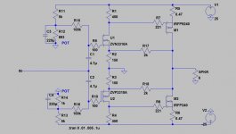
Anyway, I have come up with a schematic and modelled it (see attached). What do you think? Some questions:
1) Could this design actually work and work reasonably well?
2) Will I ever get the bias and DC offset stable? Modelling suggests just an extra ohm on the bias resistance will add many volts of DC offset. If not, can you think of an easy way to stabilise it?
3) What do you think about my choice of input stage gain and amount of feedback?
4) Any problems in general?
As usual your advice is appreciated!
Greg.
I thought I might jump on the push pull bandwagon and am contemplating building an F5 style amplifier. I don't have any suitable jfets, but I thought I might try using small mosfets for the input stage. I have a bunch of ZVN3310As and ZVP3310As lying around and thought I might try them.
While I know the jfets are superior, there are some nice sounding mosfet only amps out there too
A negative tempco in all active devices is a plus as well.Anyway, I have come up with a schematic and modelled it (see attached). What do you think? Some questions:
1) Could this design actually work and work reasonably well?
2) Will I ever get the bias and DC offset stable? Modelling suggests just an extra ohm on the bias resistance will add many volts of DC offset. If not, can you think of an easy way to stabilise it?
3) What do you think about my choice of input stage gain and amount of feedback?
4) Any problems in general?
As usual your advice is appreciated!
Greg.
Attachments
Thanks Nelson,
A question though, why do R1 and R4 need to be pots when I can set the overall bias using the pots on the input? Is it just to equalize the current in each input fet? If so, what is the importance of this? I figured it wouldn't matter if they were slightly different (which if R1 and R4 are the same will be necessary to correctly bias the output fets).
Many thanks for your advice!
Completely understandable - the diagram is by no means clear - who reads the words anyway? I put single resistors there because it was simpler to model.
So I take it I can leave R1 and R4 as is?
What are your thoughts on the effect of the unequal currents through the two input fets? Does that matter? They need to be different by about 1mA due to the differences between the p and n channel devices.
I guess the input stage gain is set by the D/S resistor ratios and the devices have pretty different characteristics anyway, should it shouldn't matter much, right?
Thanks again,
Greg.
I put single resistors there because it was simpler to model.So I take it I can leave R1 and R4 as is?
What are your thoughts on the effect of the unequal currents through the two input fets? Does that matter? They need to be different by about 1mA due to the differences between the p and n channel devices.
I guess the input stage gain is set by the D/S resistor ratios and the devices have pretty different characteristics anyway, should it shouldn't matter much, right?
Thanks again,
Greg.
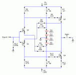
Hi Greg
Awhile ago I was playing with an F5-ish type circuit using BJTs and came up with a different biasing arrangement that might also work with mosfet input devices.
The schematic below shows the idea. Moving the bias voltages from the gates to the drains of the input devices makes things a bit simpler and gets rid of the input coupling caps.
btw: LEDs make nice, low noise voltage references and didn't seem to add much (if any) distortion, at least in sims of the BJT version.
Please don't take the values of R3, R4, R5 and R6 seriously. I'm sure they'll need to be changed.
As for adjustments, I suppose the minimum would be to make R9 and R11 adjustable, and add a trimpot between the sources of the input devices. Only problem is if that trimmer goes open circuit, that might blow your output devices. Probably better to have separate adjustments for the two input devices anyway.
Cheers - Godfrey
Attachments
... I have been unable to get this circuit to sim as well as mine ....
I would try 1k for R5 and R6, 120R for R3 and R4 and 1000uF bypass over D3,4 and another one over D1,2
R9 and R11 should be adjusted to achieve appropriate biasing of Q3,4
Gates of input MOSFETs shouldn't be directly connected to each other - some small resistance (100R) would be OK
Thank you both for your comments.
Well I must have learnt something. These are exactly the values I tried. Haven't tried bypassing the diodes though. Will try that tonight.
Thanks,
Greg.
Sounds like a good idea but I still don't really understand how it is implemented. I've looked at the F4 schematic and the biasing arrangement is beyond me. If you'd like to explain how it works it would be appreciated!Maybe use a TL431 as a bias generator ala burning amp or F4???
I would try 1k for R5 and R6, 120R for R3 and R4 and 1000uF bypass over D3,4 and another one over D1,2
R9 and R11 should be adjusted to achieve appropriate biasing of Q3,4
Gates of input MOSFETs shouldn't be directly connected to each other - some small resistance (100R) would be OK
Well I must have learnt something. These are exactly the values I tried. Haven't tried bypassing the diodes though. Will try that tonight.
Thanks,
Greg.
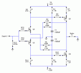
For a fair comparison, the feedback resistors should be the same in both cases. The idling current through the LEDs should also be much higher than the signal current.I have been unable to get this circuit to sim as well as mine (in terms of THD), though I have no idea why.
I think setting the bias properly would be very difficult with that circuit anyway, due to variation of Vgs between devices. The LED-based constant voltage bias works nicely for BJTs but is probably not the best for FET input devices.
The circuit below is probably better. R1 and R2 set the input stage current fairly accurately, and the bias voltages sort themselves out. To make the circuit less sensitive to changes in power supply voltage, the voltages across R1 and R2 could be zener-stabilized.
The easy way to adjust this would be to choose R1 and R2 to give the desired input stage idling current (about 8mA as shown), then use R9 and R11 to set the output stage idling current and zero offset.
That might result in unequal signal current through Q3 and Q4 though. So you might need to adjust R9 and R11 to give equal gain for both halves of the amp, and then adjust R1 and R2 for zero offset. i.e. The idling current through Q1 and Q2 may need to be different.
Attachments
Godfrey,
Thanks for your comments, and your time making those schematics.
This is how I had it set up.
Definitely had this bit wrong - only 5mA through the LED (R1 & R2), but nearly 10mA bias current through the FETs. Will try again tonight.
I like it. Will sim this one tonight too.
Thanks again Godfrey.
Thanks for your comments, and your time making those schematics.
For a fair comparison, the feedback resistors should be the same in both cases.
This is how I had it set up.
The idling current through the LEDs should also be much higher than the signal current.
Definitely had this bit wrong - only 5mA through the LED (R1 & R2), but nearly 10mA bias current through the FETs. Will try again tonight.
The circuit below is probably better. R1 and R2 set the input stage current fairly accurately, and the bias voltages sort themselves out. To make the circuit less sensitive to changes in power supply voltage, the voltages across R1 and R2 could be zener-stabilized.
I like it. Will sim this one tonight too.
Thanks again Godfrey.
Hi Greg
Time to slow down and think things through a bit. Nevermind the simulator for a moment...
In my original circuit R3 and R4 in the feedback network were 2.2K, so with an input signal swing of +-1V, the signal current through the resistors into the LEDs was about +-0.5 mA. The LED idling current was about 10mA, so variation of LED current with signal was about +-5%. Signal voltage across the LEDs was very small and distortion of that voltage was also low.
In your circuit R3 and R4 are 150R, so with the same input voltage the signal current through the resistors is about +-6mA. If the idling current through the LEDs is 10mA, the LED current will be varying by +-60%. Oops! - much higher signal voltage across the LEDs, with MUCH higher distortion.
What to do? Firstly, you can't increase the resistor values. For decent performance from the amp as a whole, you need a reasonable amount of feedback, which means you need high open-loop gain. Since this is only a 2-stage amp, there's no wiggle-room; you need high gain in the first stage and that means low resistor values (Hey, Nelson was using 10ohms).
OK, how about increasing LED current? Well, you could go up to 20mA or so and that would be a big improvement, though still not ideal. Pushing it to 100mA isn't really an option unless you want to use a handful of LEDs connected in series/parallel.
[OT]On second thoughts, I'll concede that is actually an option. It's exactly what SY did for the biasing of his "Red Light District" valve amp - so named because all the LEDs lit it up like a Christmas tree. Not my first choice though.[/OT]
The third option, as somebody pointed out earlier, is to put a big capacitor across the LEDs. This works - the capacitors reduce the dynamic impedance, so there's less voltage swing across the LEDs and much less distortion from them. However as soon as you've put the capacitors in, you may as well take the LEDs out, eliminating the LED distortion entirely. Doing so actually makes the biasing and adjustments easier too as we shall see...
~~~~~~~~~~~~~~~~~~~~~~~~~~~~~~~~~~~~~~~~
I hate to break it to you, but relying on simulations too much is a bad idea - they can be very misleading. Part of the problem is that spice models for semiconductors, especially MOSFETs, are often very bad/inaccurate. This isn't your simulator's fault, it's because the semi manufacturers can't be bothered to model their own products properly - very frustrating.
More importantly, your simulator thinks that e.g. every ZVN3310A is the same as every other ZVN3310A. This is really not true. Looking at the datasheet, it seems that for your circuit, the gate-source voltage needs to be about 2V for a typical ZVN3310A, however it could be anywhere between about 1V and 3V (IIRC). See the problem? Results with an actual circuit can be worlds apart from what the sim predicted, just because the Vgs of your MOSFET is different to what the sim thought it was.
There's two ways to cope with this:
Plan A
Design the circuit in such a way that you don't need to know or care what the gate-source voltage is. This is the main reason I prefer the circuit with capacitors in post 13 to the circuit with LEDs in post 7. With the circuit in post 13, you set the idling current and the Vgs sorts itself out.
Plan B
Buy more parts than you need, then carefully measure, match and select individual devices for your project. This approach is actually quite popular with a lot of DIYers, and also some high-end audio manufacturers.
The problem with the circuit in post 13 is that, although the voltages will sort themselves out, they will take a moment to do so, and you are likely to get a significant thump through the loudspeakers at switch-on. To deal with that you can either use a slow-start power supply, delay connection of the speakers with relays, use a bit of Plan B, or just feel lucky, build it and see what happens.
Enough for now.
Cheers - Godfrey
ps: Sorry for overly long post.
pps: The LED bias scheme worked fine for the BJT version because there's very little variation of base-emitter voltage between BJTs.
I hate to break it to you, but relying on simulations too much is a bad idea - they can be very misleading. Part of the problem is that spice models for semiconductors, especially MOSFETs, are often very bad/inaccurate. This isn't your simulator's fault, it's because the semi manufacturers can't be bothered to model their own products properly - very frustrating.
I will just note, parenthetically, that the MOSFET models in Bob Cordell's book closely conform to what we're looking for in audio applications.
Good thinking! I've been using his BJT models but didn't notice there were FETs too. You can download them from Bob's site here, Greg.
Thank you both for your comments.
Godfrey - Many thanks for outlining how that circuit works and how to improve it. There's a lot of information there for me to digest. I need to go away and think about it (and, unfortunately, sim it to see how it works).
As for the rest of your post....
I'd like to think that I am under no illusions about the accuracy of spice models. However my reasons for using them so much are this:
I am trying to learn about amplifier design with no local help available and I am yet to find a book that really covers it. There are many books that cover the basics of common source / common emitter / common base amplifiers (basic electronics books). Conversely there are many that cover the advanced aspects of amplifier design (doug self's books).
But have not found one that talks about how to get a single gain stage and add subsequent ones to produce an amplifier. Or really how to apply voltage or current feedback. Or biasing techniques. Or, essentially, how to design an amplifier from the ground up using any topology.
Bob Cordells book is the closest I have seen, but still lacking some really basic information and how to tie it all together.
As a person with limited electronics experience, who can not simply look at a schematic and understand how it works nor visualise the currents and voltages present (though I am improving), I find simulation an important tool for querying each aspect of an amplifier design to understand how it works. I really helps me and is the best teacher I have (expect for these forums and a few key websites). It teaches me things about gain and feedback that I would never have figured out otherwise without wasting hundreds of hours soldering.
As fas as THD. etc goes, well I know the figures are rubbish. But I figure the _relative_ improvements of subtle changes or one circuit over another (using the same active devices) are probably a good indication of the shortfalls or positive aspects of a circuit.
So overall it has really helped me. Months ago I was mindlessly ordering PCBs and copying known designs without a clue how they worked. I have made a JLH class a, several of the zen amplifiers and an aleph 30 and a gainclone (though admittedly, with the exception of the gainclone, none of these ever made it into final enclosures and were used for any real period of time). Now I am beginning to try my own designs. Not because I think I can do better or be original, but because I like the idea of it. And I know I can still get a sound that I like despite the superiority of other known designs. It's all good fun!
Hi Greg
Sorry if I gave the wrong impression. I agree sims are very useful, and use them a lot too. I just wanted to point out a couple of easy pitfalls to avoid.
Hmm - well really just the one; that just as two parts can be different from each other, so the part in your hand may be different to the one in the sim.
It is a bit of a steep learning curve, but you seem to be doing well. I'm not sure what to recommend in the way of books. The one I started with, and still have for reference, is "A practical introduction to electronic circuits" by Martin Hartley Jones. I don't know if it's still in print, but maybe you could find it at a library.
Regards - Godfrey
Godfrey,
Please accept my apologies. I reread my last post and it sounds far more defensive than was intended. I guess I shouldn't type messages before my morning coffee
I printed out your schematics and read your post slowly and thought about it. There is a lot of wisdom in there and I really appreciate you taking the time to write it. I understand everything you said. This has taught me a lot about biasing with ground referenced inputs that I didn't get before, but it seems so obvious now.
You were absolutely correct. I most definitely went wrong with the LED current. I upped the current to 50mA for academic purposes and things really improved.
However, your second circuit is even better. I love it. A full push pull amplifier with only 4 active devices, a few passives and active coupling. Sims nicely too! I'm going to build this one as soon as I can get my hands on some IRFP9240s.
Thanks again for your "lecture" professor.
I'm basking in the joy of the Pink Floyd Meddle CD on my other amp...unfortunately only through a single speaker though
- Status
- This old topic is closed. If you want to reopen this topic, contact a moderator using the "Report Post" button.
- Home
- Amplifiers
- Pass Labs
- Junkbox F5