Hi All,
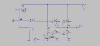
I've just designed a zero feedback current amplifier somewhat like the firstwatt F4, but a little simpler and with a single rail supply (see attached schematic). Just interested to know if there's any glaring issues or omissions or any ideas for improving the circuit?
I hope to run the amp with a tube preamp I'm also working on.
Also, any thoughts on the suitabililty of the J111 as an audio JFET? I chose it because of its high voltage capability (40V), but it looks like it really is a switching device. I was going to run it at 5mA - does that sound ok?
Any advice on the general design would be appreciated.
Thanks,
Greg.
Attachments
Last edited:
Thank you both for your replies.
"C3 can't be a .1uF? 10,000uF maybe?"
Output cap is 0.1 Farads (100,000uF). This is an experiment I thought I would try.
In one of his books Doug Self mentions an experiment he did with output capacitors on single rail amplifiers where he was able to remove essentially all output capacitor induced distortion by using an obscenely large cap (0.1F). Since I am not using feedback and have a bunch of 47000uF caps lying around I thought I would give it a go.
I could switch to a dual rail supply but I like the idea of the circuit as it is for three reasons:
1) I can test it with my cheap 0-30v, 5A lab supply.
2) No DC offset issues and a certain degree of passive speaker protection.
3) As another mentioned, current draw from the power supply needs to go through current sources to get to ground and will therefore be constant, ie Iq = Imax. I'm interested to see the effect of this. Should make life easy for the power supply I think.
So, no negative feedback so far. Looking good then.
Last edited:
Hi All,
I'm interested to know whether there would be any benefit to having a voltage regulator feeding the input buffer? I have modelled it with 1v of 100hz ripple and the increase in distortion in the input buffer is negligible so it would appear superfluous (modelled distortion goes from 0.04% to 0.042%). The jfet ccs seems to do a good job stabilising things. Would this indeed be the case?
Your advice is appreciated, as always!
Greg.
Last edited:
Problems!!
Ok,
I wired up the circuit shown in the first post using J202 jfets on the front end, with the ccs self biased at about 3.5mA. The input has a 120R gate stopper and the 240s have 221R stoppers as shown.
Sounds pretty good so far but I'm yet to make a preamp with any real voltage swing so listening levels are low. Distortion at 10kHz with my cheap 40MHz scope and FFT analysis is no higher than my signal generator....apparently.
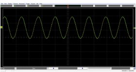
First figure shows 20kHz sinewave of input and output overlying each other. I have no idea how much distortion you need to be able to see a difference, but things are looking good so far.
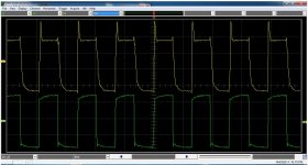
Second figure shows 20kHz square wave output (top) and input (bottom)....nasty.
Third figure shows 240 gate waveform, before stoppers (top)....nasty. Problem therefore in JFET stage I guess.
4th figure shows input to JFET after gate stopper (top).....fairly clean...no gate ringing??
So, anyone have any idea why my square waves are so terrible?
Ok,
I wired up the circuit shown in the first post using J202 jfets on the front end, with the ccs self biased at about 3.5mA. The input has a 120R gate stopper and the 240s have 221R stoppers as shown.
Sounds pretty good so far but I'm yet to make a preamp with any real voltage swing so listening levels are low. Distortion at 10kHz with my cheap 40MHz scope and FFT analysis is no higher than my signal generator....apparently.
First figure shows 20kHz sinewave of input and output overlying each other. I have no idea how much distortion you need to be able to see a difference, but things are looking good so far.
Second figure shows 20kHz square wave output (top) and input (bottom)....nasty.
Third figure shows 240 gate waveform, before stoppers (top)....nasty. Problem therefore in JFET stage I guess.
4th figure shows input to JFET after gate stopper (top).....fairly clean...no gate ringing??
So, anyone have any idea why my square waves are so terrible?
Attachments

Last edited:
Distortion?
Hi All,
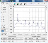
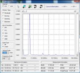
I ran the FFT module on my USB scope software using a 20kHz sinewave at approximately 9v into a 6 ohm load with a 10000uF output cap. The results are shown below in linear and db scales. I have some questions I'm hoping someone can help with.
1) Is using a FFT a valid way to test distortion? If so, is this cheap chinese software likely to do a reasonable job?
2) What can be gleaned from these figures...what do they mean in terms of THD? Can someone explain how I should interpret these figures?
3) Why the apparent lack of 2nd harmonic character?
Any info would be great. Also still keen to hear some feedback on the problem I mentioned in the above post!
Thanks,
Greg.
Hi All,
I ran the FFT module on my USB scope software using a 20kHz sinewave at approximately 9v into a 6 ohm load with a 10000uF output cap. The results are shown below in linear and db scales. I have some questions I'm hoping someone can help with.
1) Is using a FFT a valid way to test distortion? If so, is this cheap chinese software likely to do a reasonable job?
2) What can be gleaned from these figures...what do they mean in terms of THD? Can someone explain how I should interpret these figures?
3) Why the apparent lack of 2nd harmonic character?
Any info would be great. Also still keen to hear some feedback on the problem I mentioned in the above post!
Thanks,
Greg.
Attachments
Those 20 KHz square waves are not a problem. From the
looks of it, the jittery may be your test equipment.

Thanks Nelson,
I would never have suspected that as the waves look reasonable when the scope is attached directly to the signal generator before the 4.7uF poly input capacitor. If that's the case than the FFT analysis is also going to be pretty useless I would suspect!
Are you suggesting the equipment is inferior or that I am using it incorrectly?
Both are probably true.
I have a conventional CRO too, unfortunately also a cheapie. Will hook it up tonight and see how things look.
Thanks for your comments.
Greg.
Hmm,
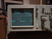
As promised, different sig gen and CRO. Same problem (see photo).
The droopy tail end of the square wave is due to the cheap sig gen and its square wave looks a lot like that anyway. But as far as I can tell the peak at the front of the wave is due to the amplifier.
Gate waveform at jfet input is perfect.
Waveform going into 240 gate stoppers is terrible. If I had ringing at the 240 gates, would this be the case or would I only see bad waveforms after the gate stoppers? Maybe I need bigger gate stoppers here?
Problem is probably in JFET input or CCS. But where and why? PCB layout is pretty good I would think.
Is this something I can fix or am I asking too much of such a simple circuit?
Should I just not bother trying to solve it given that no audio signal will have this kind of rise time?
Thanks again for your help!
Attachments
Hi Greg
Aside from the spikes, it looks like you have a nice fast rise time, but relatively slow fall time (although still enough for audio imho). Some possible problems I can think of:
a) C1 in the CCS looks (to my fading eyes) like 0.001uF i.e. 1nF. In conjunction with R5, that's going to slow things down a bit. As an experiment I would try reducing that to maybe 100pF and see what happens to the square wave.
b) The current through J2 may not be high enough to switch off M4 and M5 fast enough. You can measure the voltage across R15 to see what it's idling at. If you put a small resistor in series with J1's drain, you can check the voltage across it with a scope during the square wave test to see if it's clipping i.e. switching off during part of the cycle. Maybe you'll see something that sheds light on the other misbehavior as well.
Another limiting factor may be that there's only about 3mA of current available through R8 and R11 to drive M1 and M2. With fast output voltage swings, M1 and M2 will require quite a bit of gate current due to their gate-drain capacitance.
You could try dropping R8 and R11 to maybe 2.2K each and see what happens. Putting a small resistor in series with Q3's emitter and checking the voltage waveform across it with a scope might also give you a better idea what's going on there.
Cheers - Godfrey
p.s. I wonder how constant the current through J2 actually is. You could check the voltage across R15 with a scope to find out.
Thanks Godfrey,
I've been waiting for someone to give me some solid feedback about this for a while. Really appreciate your input. Comments below:
Yes you read correctly. Good idea, I'll make it smaller.
I was wondering about this. The CCS is biased at 3.5mA which doesn't sound like much. However it is comparable to the bias of each half of the LTP in the Aleph J so I thought it would do.
Good idea. I'll try these things and let you know how it goes. I have been wondering how to tweak the resistors values in the current source and your explanation has helped me understand it better.
It's about 3.5mA.
Will report back tomorrow hopefully.
Thanks again,
Greg.
I've been waiting for someone to give me some solid feedback about this for a while. Really appreciate your input. Comments below:
a) C1 in the CCS looks (to my fading eyes) like 0.001uF i.e. 1nF. In conjunction with R5, that's going to slow things down a bit. As an experiment I would try reducing that to maybe 100pF and see what happens to the square wave.
Yes you read correctly. Good idea, I'll make it smaller.
b) The current through J2 may not be high enough to switch off M4 and M5 fast enough. You can measure the voltage across R15 to see what it's idling at. If you put a small resistor in series with J1's drain, you can check the voltage across it with a scope during the square wave test to see if it's clipping i.e. switching off during part of the cycle. Maybe you'll see something that sheds light on the other misbehavior as well.
I was wondering about this. The CCS is biased at 3.5mA which doesn't sound like much. However it is comparable to the bias of each half of the LTP in the Aleph J so I thought it would do.
Another limiting factor may be that there's only about 3mA of current available through R8 and R11 to drive M1 and M2. With fast output voltage swings, M1 and M2 will require quite a bit of gate current due to their gate-drain capacitance.
You could try dropping R8 and R11 to maybe 2.2K each and see what happens. Putting a small resistor in series with Q3's emitter and checking the voltage waveform across it with a scope might also give you a better idea what's going on there.
Good idea. I'll try these things and let you know how it goes. I have been wondering how to tweak the resistors values in the current source and your explanation has helped me understand it better.
Cheers - Godfrey
p.s. I wonder how constant the current through J2 actually is. You could check the voltage across R15 with a scope to find out.
It's about 3.5mA.
Will report back tomorrow hopefully.
Thanks again,
Greg.
Godfrey,
As promised I have made some modifications to the circuit. I didn't have a 100pf cap for the ccs cap so I removed it completely. Spikes gone! This causes me to ask, what is the purpose of this cap anyway, and do we really need it?
I also dropped R8 and R12 to 2.5k, but performance is much the same.
Unfortunately the droopy tail is still there, but I think it is probably from too little current in the input stage ccs, as you suggested. I will try replacing the bottom J202 with a J203, which has a much higher current flow at Vgs=0. Unfortunately I don't have any on hand so we will have to wait a week or two.
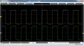
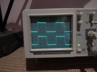
Here is a scope shot of a 20kHz square wave. Top trace is the input into the top JFET. Bottom trace is the output waveform across a 6R load and through a 10,000uF output cap. A big improvement. As you can see my sig gen isn't exactly a great performer either.
Obviously when unloaded the rise time looks a little better, but the unloaded output isn't what counts, is it?
Thanks again for your help. This has been a very educational experience.
As promised I have made some modifications to the circuit. I didn't have a 100pf cap for the ccs cap so I removed it completely. Spikes gone! This causes me to ask, what is the purpose of this cap anyway, and do we really need it?
I also dropped R8 and R12 to 2.5k, but performance is much the same.
Unfortunately the droopy tail is still there, but I think it is probably from too little current in the input stage ccs, as you suggested. I will try replacing the bottom J202 with a J203, which has a much higher current flow at Vgs=0. Unfortunately I don't have any on hand so we will have to wait a week or two.
Here is a scope shot of a 20kHz square wave. Top trace is the input into the top JFET. Bottom trace is the output waveform across a 6R load and through a 10,000uF output cap. A big improvement. As you can see my sig gen isn't exactly a great performer either.
Obviously when unloaded the rise time looks a little better, but the unloaded output isn't what counts, is it?
Thanks again for your help. This has been a very educational experience.
Attachments
Last edited:
Ah crap! I hooked it up to my other sig gen (a slightly better one) and unregulated PSU, and the peaks are back. Nowhere near as bad as before, but they're there. On a positive note the rise time is much better with the unregulated PSU. Seems the regulated one is too slow.
Last edited:
Wow, that was fastAs promised I have made some modifications to the circuit.
You're asking me? I didn't put it there!...what is the purpose of this cap anyway, and do we really need it?
OK, seriously; a small cap may be needed for stability - in your case it seems not. Anyway a cap that big looks like someone was deliberately trying to slow it down a bit. Thinking about it, the cap decides how fast the CCS wants to react, but the current through R8 and R11 decides how fast it can react.
Can't you just reduce the value of R15 to increase the current?I will try replacing the bottom J202 with a J203, which has a much higher current flow at Vgs=0.
Any sig gen and scope is better than none. All I have these days is a multimeter.As you can see my sig gen isn't exactly a great performer either.
The acid test is loading the output with small capacitors, say 1nF to 10nF. That's what really hurts stability. Don't do like Carlos and blow up your amp trying to drive full power square waves into a 100nF cap though.Obviously when unloaded the rise time looks a little better, but the unloaded output isn't what counts, is it?
Hi Greg,
Out of curiosity; have you tried using the positive rail as reference for the input as well (with C5 across R1 instead of R2)?
Also how is the layout of the positive rail done? Where is the speaker return connected? Close to M4, M5?
Hi tsz,
No I haven't tried that. Is there any reason to?
The speaker return is connected to ground (unlike the schematic).
The PCB layout is attached (but I'm only using 2 output pairs, not 3).
Attachments
- Status
- This old topic is closed. If you want to reopen this topic, contact a moderator using the "Report Post" button.
- Home
- Amplifiers
- Pass Labs
- My take on the F4 - advice needed