If you read the data from Fischer a bit further down you see :
Thermal resistance: 0,07 K/W .....
Thermal conductivity: 0,45 W/mK
0.45 W/mK is the material constant.
0.07 K/W refers to that particular insulator with a specific surface geometry.
Rth Kapton Bulk = 0.45 x 0.00005 / (0.024 x 0.021) = 0.045 K/W for a TO247 Insulator.
But this is the resistance of the bulk material itself.
On top of that you need to add the Thermaphase conductive layer on both sides.
What that is precisely and how to arrive at the 0.32 extra resistance is not explained by Fischer.
I presume you then do not need to add grease with that stuff already coated.
I am still using Kerafol.
You only need to measure temperature difference between MOSFET case and heat sink with the same device dissipating the same heat
to figure out which is better and by how much.
As I mentioned elsewhere before, the thermal prediction for my AX100 agrees with measurement to <2°C, over the total thermal chain.
And no, I don't have share at Kerafol.")
Patrick
Thermal resistance: 0,07 K/W .....
Thermal conductivity: 0,45 W/mK
0.45 W/mK is the material constant.
0.07 K/W refers to that particular insulator with a specific surface geometry.
Rth Kapton Bulk = 0.45 x 0.00005 / (0.024 x 0.021) = 0.045 K/W for a TO247 Insulator.
But this is the resistance of the bulk material itself.
On top of that you need to add the Thermaphase conductive layer on both sides.
What that is precisely and how to arrive at the 0.32 extra resistance is not explained by Fischer.
I presume you then do not need to add grease with that stuff already coated.
I am still using Kerafol.
You only need to measure temperature difference between MOSFET case and heat sink with the same device dissipating the same heat
to figure out which is better and by how much.
As I mentioned elsewhere before, the thermal prediction for my AX100 agrees with measurement to <2°C, over the total thermal chain.
And no, I don't have share at Kerafol.
Patrick
Last edited:
Other then long cable runs, what is the point behind balanced pre amps and power amps. If that is the only reasoning what is considered a long run for either a f5 or f5x, or even a f5t. I don't know if this question should be else where if so it may be moved, sorry for any hijacking of this thread.
Why not search in Google for a more balanced opinion ?
Patrick
Is that a play on words,
Patrick,
While studying the history of source generation in the context of the F5 amp I came over this post in the F5 thread where you present your build F5X (for the first time?).
You say:
"Circuit is similar to the balanced version posted by Tino.
Rails are +/- 16V, total bias 4A.
JFETs are matched 2SK170BL/2SJ74BL running at 5mA.
Output MOSFETS are 2SK1530/2SJ201.
Source resistor 0R22 & 0R18 respectively."
Would that mean that you were biasing the K1530/J201 differently to make the devices track better and why did you give it up later?
Nic
It meant that I was using a different way than in the public version to take care of the different Yfs of the JFETs.
The public version is much easier to understand and hence to build.
The end results are, at least in theory, the same, i.e. open loop gain balancing between top & bottom halves.
Patrick
The public version is much easier to understand and hence to build.
The end results are, at least in theory, the same, i.e. open loop gain balancing between top & bottom halves.
Patrick
Thanks Patrick - I'm learning and that is important (for me)
>It meant that I was using a different way than in the public version to take care of the different Yfs of the JFETs.
Essentially you are compensating the non-complementarity of the K170/J74 FETs using different source degeneration for the K1530/J201. In the later public version this is replaced by differential degeneration directly on the JFET's (typically 10R/15.1R). Correct?
>The public version is much easier to understand and hence to build.
I disagree. It is generally easier to build that to understand. Anyway, the use of different MOSFET source resistors is not really that easy to understand without an explanation, but then again I may be a very dumb audio DIY'er
>The end results are, at least in theory, the same, i.e. open loop gain balancing between top & bottom halves.
I'm very happy to hear that
It seem that a proper source R choice is a reliable way to compensate off-sets in both JFET and MOSFET complementarity.
Cheers,
Nic
P.S. Out of complete ignorance with respect to audio terminology: does "top & bottom" effectively equal "front-end & output-stage" ?
Top & bottom means +ve rail and -ve rail halves.
The use of different source resistor values have already been mentioned once when we discussed poor NN-PP match before.
You need to calculate the total open loop gain from front to end (in this case only 2 stages).
Changing one resistor values will force other changes to occur simultaneously.
And that has to be taken into account.
That applies to the first order effects (one assume the FETs to be linear).
When you take higher orders into account, it becomes more complex.
Writing some equations will help you to figure it out.
Or learn to use Spice and play with the model.
Patrick
One more comment I want to make about how to compensate for the difference between K170/J74 Yfs.
In my first build, I calculated the combined open loop gain of the first & second stages of the top & bottom halves respectively and balanced them by adjusting the value of the MOSFET source resistor as well as the feedback resistor network values.
I have in the public version changed that approach, not only because it is more complex to calculate and understand, but also for philosophical reason. The current design philosophy is that any "error" should be corrected for locally where they occur. And since the 2SK1530/2SJ201s are perfect complementaries, the correction is only done at the front end, namely the 5R extra degen for the 2SJ74s.
The same approach is used for the F5XP, for example. In this case, the first stage also has the 5R degen for the 2SJ74. So the gain of the first stage is balanced. The second stage also has an imbalance between the 2SK216 and 2SJ7 both in Yfs and in Vgs, and this is then compensated by adjusting the source resistor values.
The advantage of this more laborious approach is that if one day we find a perfect complementary pair of TO220 devices, we can take out the Renesas laterals and subsititute these in, but then with equal source resistor values.
i.e. if each stage is individually balanced, you can change one without affecting the other.
As said, it is a philosophical thing. There is no proof if one sounds better than another.
What I said in post #1 ?
100 ways t skin a cat.
Patrick
Last edited:
Today I powered up one of my amp modules
330mV after 2:30 hours, -20V/+19,98 supply
190mV offset on negative side 90mV on positive (to ground)
need I to do an adjustment like the regular F5 for get the lowest offset on each side?
An externally hosted image should be here but it was not working when we last tested it.
330mV after 2:30 hours, -20V/+19,98 supply
190mV offset on negative side 90mV on positive (to ground)
need I to do an adjustment like the regular F5 for get the lowest offset on each side?
> 330mV after 2:30 hours, -20V/+19,98 supply
Measured after CRC ?
Sounds high; what is the bias current ?
> need I to do an adjustment like the regular F5 for get the lowest offset on each side?
Yes.
But perhaps better to post at the build thread and continue from there ....
http://www.diyaudio.com/forums/pass-labs/208880-f5x-euvl-approach-build-thread.html
Patrick
As promised.
Patrick
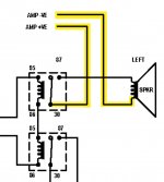
From the diagram attached to post #706.
I see VE + and - for left speaker are connected to the same pole?
I do not quite understand the question.
I checked the diagram and cannot spot any mistake around the left speaker.
The only thing is that Mark (who drew the schematics) was using 12V relays, so he wired the left & right protection relays in series.
Maybe you can explain further ?
Patrick
I checked the diagram and cannot spot any mistake around the left speaker.
The only thing is that Mark (who drew the schematics) was using 12V relays, so he wired the left & right protection relays in series.
Maybe you can explain further ?
Patrick
- Status
- This old topic is closed. If you want to reopen this topic, contact a moderator using the "Report Post" button.
- Home
- Amplifiers
- Pass Labs
- F5X -- the EUVL Approach