Finally, a question I can answer!I have a question that I am sure someone can answer. Why do you P-channel devices always (well at least it seems that way) have higher levels of input capacitance to their N-channel complement.
The real answer is that to produce "matching" (complementry) FETs with the same RDSon, the P-channel device is 2.5 to 3 times bigger than the N-channel device. Bigger silicon area......... More gate capacitance.
Rds is dependent on the Current Ids which is given by equation
Ids = (uCi/2) (W/L) (Vgs - Vth) (Vgs-Vth)
u is the electron mobility.
Mobility of n-type carriers (electrons) is ~ 2x mobility of p-type carriers (holes).
To match a P-channel Ids to a N-channel Ids, the input capacitance of the P-channel must be ~ 2x the input capacitance of the N-channel.
Not really "bad dope during doping process"
.....
Not really "bad dope during doping process"

now you ruined my perception of Universe .........

") I looked at Bob Cordells book for the deepness of outputstage...
I looked at Bob Cordells book for the deepness of outputstage...I found only one sentence to give more information than you all did....
"A greater number of output transistors relaxes thermal concerns,
improves thermal stability, and makes the amplifier performance less vulnerable
to beta droop effects."
what are beta drop effects? Here comes the answer...from Bob Cordell:
"Beta Droop
The current gain of power transistors tends to fall off rapidly above a certain collector
current. This is called beta droop. While a power transistor might have a beta of 80 at
1 A, the beta might fall to 20 or less at a collector current of 10 A. This makes it much
harder for the amplifier to deliver high current to the load. This can also endanger the
driver transistor because it will be asked to supply very high base current to the output
transistor."
May be this is one of the reasons why Nelson uses so many stages even in XA30.5...
Beta Droop is a BJT transfer curve function and is not quite the same with MOSFETs
The current gain of power transistors tends to fall off rapidly above a certain collector
current. This is called beta droop. While a power transistor might have a beta of 80 at
1 A, the beta might fall to 20 or less at a collector current of 10 A. This makes it much
harder for the amplifier to deliver high current to the load. This can also endanger the
driver transistor because it will be asked to supply very high base current to the output
transistor."
May be this is one of the reasons why Nelson uses so many stages even in XA30.5...
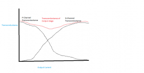
When Bob says Beta Droop. I am almost certain he is referring to transconductance droop at the crossover point for an under biased mosfet outptut stage
Unlike us, I think Bob's philosophy is to bias as low as possible while still maintaining good THD through the use of error correction.
We are at the other extreme - bias the hell out of it and make the amp as linear as possible so you don't need to use error correction in the first place. That is how I see it anyway - known as the KISS principle.
Last edited:
I beleive he is refering to the "Beta" curve peaking and subsequently dropping at higher currents.When Bob says Beta Droop. I am almost certain he is referring to transconductance droop at the crossover point for an under biased mosfet outptut stage

I agree with that.
The absolute minimum beta/transconductance droop occurs at the crossover point for an under biased mosfet output stage.
Edit: Actually I think I disagree. Not disagree with your statement regarding bipolars, but what he is referring to with mosfets.
The absolute minimum beta/transconductance droop occurs at the crossover point for an under biased mosfet output stage.
Edit: Actually I think I disagree. Not disagree with your statement regarding bipolars, but what he is referring to with mosfets.
Last edited:
Well, from another thread:
I don't condone the post txt, as I think I was being stepped on by someone with an unwarrented condesending attitude (who has not responded, yet). However, what he sitted is good for this discussion. Choose
Learning more about the subject will do you good:
http://www.diyaudio.com/forums/pass-labs/129040-mosfet-output-stage-capacitance.html#post1599135
I don't condone the post txt, as I think I was being stepped on by someone with an unwarrented condesending attitude (who has not responded, yet). However, what he sitted is good for this discussion. Choose
thanks flg for your hint....
I found your post from 2008
http://www.diyaudio.com/forums/pass-labs/129040-mosfet-output-stage-capacitance.html#post1599135 look for post #5 from flg
it seems that an output stage with a greater deepness works better in Class AB than a single or less devices.
Seems Nelson compensates leaving earlier class A than with the Aleph series in this way....
but I know with my small knowledge it is a keen statement.....
and maybe Andrew wanted to say me the same.....
I found your post from 2008
Being not unlike other DIYer's, I also did the same sims with a 20V Pk output. Note, that we are now entering Class AB territory.
The 4 pair circuit measures .092% THD @1kHz. The Gate current for each N FET measures about 30uA (Pk) and the Ps about 28uA.
The single pair circuit measures .165% THD @1kHz (including 2nd, 3rd, a little 4th, 5th and 7th). It's gate current is about 32uA into the N and P gates.
More questions???
http://www.diyaudio.com/forums/pass-labs/129040-mosfet-output-stage-capacitance.html#post1599135 look for post #5 from flg
it seems that an output stage with a greater deepness works better in Class AB than a single or less devices.
Seems Nelson compensates leaving earlier class A than with the Aleph series in this way....
but I know with my small knowledge it is a keen statement.....
and maybe Andrew wanted to say me the same.....
- Status
- This old topic is closed. If you want to reopen this topic, contact a moderator using the "Report Post" button.
- Home
- Amplifiers
- Pass Labs
- deepness of outputstages