I just measured DC offset with P1/P2 at zero ohm and couldn't believe what I saw, -21V.
Check voltage across jfet source resistors. If they look good(6-8mA range), then trying biasing ouput again. Just because you adjust one without a reaction does not necessarily mean cooked anything. One ouput fet may require higher Vgs for same bias level. In that case lower Vgs part will show signs of biasing on, while higher Vgs fet, will seem to do nothing. The F5 is about balance. Sort of tug of war between output fets. If all is good, they push and pull together. If something is off, then one side is stronger, takes control, and throws off balance. You may have been bad fet, but not necessarily.
Well Jim, measuring resistance of 18 ohm on the far side of the gate R14 100 ohm resistor made it clear that N ch MOSFET was bad. I don't think I burnt it but it probably came bad from the supplier. Or static killed it I really don't know. Anyhow I replaced the N ch MOSFET (IRFP240) and all seems good for now. However, I still see both JFETs running quite hot when I turn P1/P2 slowly. How hot should they be in normal operation? I shouldn't jump to any conclusion yet, but I am not too convinced that J111/P1086 I am using are suitable for this application. It is getting late and I don't want to start adjusting BIAS so late. Will do it tomorrow morning. Jim if you could bring a pair of K170/J74 tomorrow when we meet for lunch that would be great. Let me know if you need anything from me to bring. thanks again Jim
Check voltage across jfet source resistors. If they look good(6-8mA range), then trying biasing ouput again. Just because you adjust one without a reaction does not necessarily mean cooked anything. One ouput fet may require higher Vgs for same bias level. In that case lower Vgs part will show signs of biasing on, while higher Vgs fet, will seem to do nothing. The F5 is about balance. Sort of tug of war between output fets. If all is good, they push and pull together. If something is off, then one side is stronger, takes control, and throws off balance. You may have been bad fet, but not necessarily.
thanks buzzforb. I think I nailed down the problem to N ch MOSFET. Next will be to see how close are the JFETs matched. Jim said you have some JFETs/MOSFETs for sale. Could you PM me pls with a list of what you have. thanks
")
thanks buzzforb. I think I nailed down the problem to N ch MOSFET. Next will be to see how close are the JFETs matched. Jim said you have some JFETs/MOSFETs for sale. Could you PM me pls with a list of what you have. thanks
Sure. Whatdid you measure across the 10R source resistors of the jfet. It will tell you the amount of current passing through each of them. You msy have nailed down the mosget problem, but lets invedtigate the jfet problem.
For the F5 R1 is that R3/R4?Check voltage across jfet source resistors...
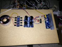
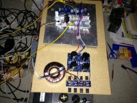
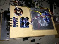
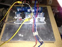
Hey guys, buzzforb is right, my JFETs were taking way too much current so rather then re-designing the source resistor network, today I met for lunch with my friend Jim (6L6). He brought a pair of almost perfectly matched K170/J74, so today was my day of fun indeed. Once I put those JFETs in the circuit, adjusting the BIAS was a breeze. Started from 0 ohm, but I could have started from 3-4 turns on P1/P2 each. They started 'catching' at about 5-6 turns. At about 7-8 turns I adjusted BIAS to about 0.5V and the R3/R4 voltage drop was about 4.2V, like on the original schematic. DC offset was about 35-40mV, which I think is great. Since I don't have the large heath sinks mounted yet (see pics) I didn't want to push BIAS over 1.2A yet, but I will once the amp is built. Then I did a quick audio test with CJ PV14 as a pre-amp (tube), before the MOSFETS got too hot and the amp sounded outstanding. Next will be to do some measurements now that I have 2 good working modules. Many thanks to my friend Jim who provided me with the JFETs. Like someone said before, if you have a good matched set of JFETs, adjusting this amp is a snap. I'll post some pictures once I figure out how to attach them. thanks Jim, thanks buzzforb
Attachments
Last edited:
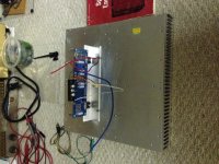
F5 first proper audio test
Today I did the first proper stereo audio test with my newly built F5 stock modules. The amp modules were mounted on a proper 300mm x 300mm heatsink and left to warm up for 1 hour. The heatsink was warm but not too hot after an hour. At first I thought that the amps lack on bass, but when I played Pink Floyd Money and Wish You Were Here, it became apparent that these amps do sound fantastic, crisp and with no coloration of any kind. I am really impressed. I am still to play some classical music and my fav FLAC digital files. Now my dilemma is should I just stick with these stock F5s and finish building them, or opt for a balanced version which will put out more power. I seem to need a bit more power at least with CJ PV14 as a pre and my 12" Altec woofers and Goodmans enclosures, but I should try them with X2.5 and Aleph P and also with UGS pre, which I am yet to finish the case for. Stay tuned for my build thread.
Today I did the first proper stereo audio test with my newly built F5 stock modules. The amp modules were mounted on a proper 300mm x 300mm heatsink and left to warm up for 1 hour. The heatsink was warm but not too hot after an hour. At first I thought that the amps lack on bass, but when I played Pink Floyd Money and Wish You Were Here, it became apparent that these amps do sound fantastic, crisp and with no coloration of any kind. I am really impressed. I am still to play some classical music and my fav FLAC digital files. Now my dilemma is should I just stick with these stock F5s and finish building them, or opt for a balanced version which will put out more power. I seem to need a bit more power at least with CJ PV14 as a pre and my 12" Altec woofers and Goodmans enclosures, but I should try them with X2.5 and Aleph P and also with UGS pre, which I am yet to finish the case for. Stay tuned for my build thread.
Attachments
Great!!
How big is your transformer? Are you at full bias?
You do have the heatsink for a Balanced F5...
The toroid is 350VA (18+18VAC), if I decide to go balanced I will have 2nd PS and the toroid. The rectifier diodes I am using were only warm after 4-5 hours of use and I don't think they need a heathsink. My BIAS is at 1A right now. I think I read the recommended BIAS for a single MOSFET pair is 1.3A per side, but what is the max you can get out of this design? I would like to max it out because I have enough heathsinks to do that. The reason I want to try maxing out the BIAS is to see if there is any sound difference with BIAS at the max.
i would not go over around 35W dissipation pr fet. With 23V rails, that comes down to:
35W/23V=1.52A bias. Your sinks is from heatsinkUSA With 0.33"(9mm) base plate?
the sinks are effective in a radius of 10x the base thickness. rest of the sink will be pretty much useless.
35W/23V=1.52A bias. Your sinks is from heatsinkUSA With 0.33"(9mm) base plate?
the sinks are effective in a radius of 10x the base thickness. rest of the sink will be pretty much useless.
i would not go over around 35W dissipation pr fet. With 23V rails, that comes down to:
35W/23V=1.52A bias. Your sinks is from heatsinkUSA With 0.33"(9mm) base plate?
the sinks are effective in a radius of 10x the base thickness. rest of the sink will be pretty much useless.
Acquired heathsinks from a local parts store and I think they came from a local RF factory, they were designed for RF amps. The base is about 1/2" thick, and the heathsink was evenly warm but not burning hot after 4-5 hours of use. Thanks for the max dissipation value of 35W per side. Using that value I can calculate my max output voltage swing: 35W / 8 ohm ~ 2A, so 2 x 8 = 16V. Is this correct (simplistic) way to calculate the voltage swing for max dissipation?
no.
he stated <=35W per device, not per side.
A ClassA Push Pull amplifier can deliver ClassA output current up to 2times the output stage bias current.
If the bias is set to 1.3A, then maximum current in ClassA is 2.6Apk.
Voltage swing across a 8r0 load would be 2.6*8=20.8Vpk
he stated <=35W per device, not per side.
A ClassA Push Pull amplifier can deliver ClassA output current up to 2times the output stage bias current.
If the bias is set to 1.3A, then maximum current in ClassA is 2.6Apk.
Voltage swing across a 8r0 load would be 2.6*8=20.8Vpk
Guys, just to let you know that I am looking into ways to push F5 into class AB without much circuit change, with less power, heath and BIAS current. Has anyone thought of bumping up PS to +-40-45V and adding another BJT driver stage and reducing FET BIAS to ~150mA, or something along those lines? Spent most of the weekend in bed sick, reading about class AB and I like it a lot. There is tons of material on the web and in diyaudio, but has anyone tried to convert F5 to class AB, without heavy lifting?
- Home
- Amplifiers
- Pass Labs
- How to build the F5