Juma,
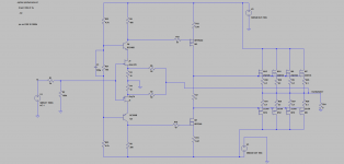
Thanks for the PCB layout. For the rest of the thread: Juma designed the layout and I added the cascode bits.
I'm using the 3W 150s because I'm not sure whether I want 50 ohms at the end of the day or 75 ohms for feedback. With the 3W version, I have the choice. The crowding is easily solved by using two layers (I'll take a pic from the side to show this).
@NYCOne
I look at your PCB in post #1 and it's a bit crowded with 150R/3W feedback resistors.
I planned that PCB for 3x150R/2W feedback resistors since I can't buy locally 100R/3W ones.
You can use 2x100R/3W to avoid crowding.
O.K. I have some time. I don't know exactly where people are having trouble but, lets see if I can shed some light on the F5 case of input cascode modification. Basically we can read about the benifits elsewere, as in the previous sited papers authored by N.P. or Borbely etc. I will just try to squeeze in a cascode device as designed into the CViller boards I have (rev2 I guess). The schematic can be found here diyAudio - cviller go down to F5. I'm sure if you only want to know what time it is, you should skip to the next post.
We will be maintaining something very close to the original qurrent through input JFETs Q1,2 but, we will place the emitter of the selected Bipolars Q101,102 to the drain of the JFETs through a second hole provided on the PCB and marked "casc" I believe. No change in the JFETs 10 ohm source Rs is necessary.
Pictured in most of these cascoded F5 schematics is a voltage divider from each rail to Gnd or maybe from rail to rail(R101,102,103,104 in CVillers board). I think in almost all the schematics I've seen, the voltage divider is setting up 1/2 of the rail voltage as a refrence for the cascode. That might be O.K. but, I seem to remember some of these "experts" saying these JFETs work the best at around 8-10Vds so thats where I would put my ref voltage. The drain of the input JFETs will see about .6V less than the refrence voltage you set at the base of Q101 and 102. It is a personal choice based not only on where you want the JFETs to operate but also what the rail voltage is. In the case of a 2X25VRMS xfrmer giving about 32-33V rails I would want my voltage divider to provide about 25% of the rail voltage to the base of the Cascode xistor. So where CViller and N.P. and others have 2 equal value restors in the R101,102,103,104 position you might get 16.5V at the base of Q101,102. Me though, I think I would use more like a 12k for R101,103 and a 4k for R102,104 giving me about 8V at the base of Q101,102. A reasonable limit for the JFETs Vds is probably around 20V due to the power dissapation it will inccur with 5mA through it. I think any more than about 100mW is starting to push it a little.
I think what I have described would be just fine for the 32-33V rail situation without any other changes than adjusting P1,P2 as normal. Hopefully I'm getting this discussion rolling a little. I have undoubtedly overlooked things, dare I say due to my intelegence but, I'm open for further questions, ideas, etc...
I'll give you an example:
On the Balanced thread I asked about NTC thermistors. I was trying to decide what to buy. I was concerned about the steady state current being too high for the CL-60s NP used in the stock F5 (http://www.diyaudio.com/forums/pass-labs/172770-balanced-f5-question-74.html#post2411412 see post 735).
Instead of getting an answer, I was directed to search the internet (which I'd already done) or buy a book. The suggestion was there were numerous threads that already answered the question. If there were, I either didn't find them, or didn't think they answered the question for the Balanced F5.
NP ultimately answered the issue in one sentence. In my opinion, that's the sign of a true expert, one who is willing to spend the time to answer questions, even if they are simple compared to one's knowledge.
I happen to be a member of that "private club" and I can say that it is not as exciting as you think it is. All of the schematics are either public relatively straight forward or could be dangerous in the current state. We are just not very fast and are working on our own. There is just not that much to see.
Alexis Shaw
Which would give the better outcome, caps around each cascode grounded, or a cap between the bases linking them together. It's a trivial matter to re-etch a board.
That would be the "fewer parts" edition. The cap from
base to base achieves much the same thing as the base
currents cancel each other.
This is a bandwidth issue, the object being to prevent
the cascodes from degrading the bandwidth due to high
impedances on their bases.

Maybe, but if NP is willing to opine, I will re-etch, the best is the best...
you'll need golden ear to hear difference
Yes, but I'd hope someone has already run the experiment. It would save a lot of time if there is an answer.
You suggest the answer may be too close to call, if that's the case, then no re-etching needed.
You suggest the answer may be too close to call, if that's the case, then no re-etching needed.
feel free to re-etch , than opine by your self
only that is valid
This was a great explanation of the cascode. Personally, I appeciate the effort.
O.K. I have some time. I don't know exactly where people are having trouble but, lets see if I can shed some light on the F5 case of input cascode modification. Basically we can read about the benifits elsewere, as in the previous sited papers authored by N.P. or Borbely etc. I will just try to squeeze in a cascode device as designed into the CViller boards I have (rev2 I guess). The schematic can be found here diyAudio - cviller go down to F5. I'm sure if you only want to know what time it is, you should skip to the next post.
We will be maintaining something very close to the original qurrent through input JFETs Q1,2 but, we will place the emitter of the selected Bipolars Q101,102 to the drain of the JFETs through a second hole provided on the PCB and marked "casc" I believe. No change in the JFETs 10 ohm source Rs is necessary.
Pictured in most of these cascoded F5 schematics is a voltage divider from each rail to Gnd or maybe from rail to rail(R101,102,103,104 in CVillers board). I think in almost all the schematics I've seen, the voltage divider is setting up 1/2 of the rail voltage as a refrence for the cascode. That might be O.K. but, I seem to remember some of these "experts" saying these JFETs work the best at around 8-10Vds so thats where I would put my ref voltage. The drain of the input JFETs will see about .6V less than the refrence voltage you set at the base of Q101 and 102. It is a personal choice based not only on where you want the JFETs to operate but also what the rail voltage is. In the case of a 2X25VRMS xfrmer giving about 32-33V rails I would want my voltage divider to provide about 25% of the rail voltage to the base of the Cascode xistor. So where CViller and N.P. and others have 2 equal value restors in the R101,102,103,104 position you might get 16.5V at the base of Q101,102. Me though, I think I would use more like a 12k for R101,103 and a 4k for R102,104 giving me about 8V at the base of Q101,102. A reasonable limit for the JFETs Vds is probably around 20V due to the power dissapation it will inccur with 5mA through it. I think any more than about 100mW is starting to push it a little.
I think what I have described would be just fine for the 32-33V rail situation without any other changes than adjusting P1,P2 as normal. Hopefully I'm getting this discussion rolling a little. I have undoubtedly overlooked things, dare I say due to my intelegence but, I'm open for further questions, ideas, etc...
Thx NYCOne. As I said there are things I left out. My description was a little biased towards only raising the rail voltage and choosing to cascode to protect the input and attempt to lower distortion. Many here are interested in pairs or triplets of output devices also. This would be necessary due to the increased power dissapation of a higher rail but, a convinient method to increase output power also. Trouble is, it takes more current to drive the extra xistor capacitances or the high frequency's will suffer. Cascoding the input JFETs can help in this case also. Raising the Iq of the input stage should help in this regard. If I maintain 8Vds on Q1,2, I can easily operate the first stage at 12.5mA instead of 5mA In this situation an acompanying change in the R3,4 to some lower value. This however may cause a problem with lower input stage gain. Multiple output transistors will however increas output stage gain. These tradoffs are very likely to cause a change in the sound?
It would save a lot of time if there is an answer.
maybe there is none
the cascode does nothing else than what its supposed to do, "sharing" the voltage
theres is nothing to hear
and thats what have been stated
it works, and is inaudible
flg, your evaluation is interesting
These tradoffs are very likely to cause a change in the sound?
Change in sound is not necessarily a bad thing - Hence the reason for F1 to F5, as well as Aleph J, J2, M2, they all sound different.
It's ok to be different.
are you talking Aleph design now, I wonder
actually there are IRF TO-220(AB) with quite high transconductance, if thats requested
http://docs-europe.electrocomponents.com/webdocs/0dcb/0900766b80dcb1be.pdf
http://docs-europe.electrocomponents.com/webdocs/0791/0900766b807910f2.pdf
http://docs-europe.electrocomponents.com/webdocs/0791/0900766b807910ff.pdf
http://docs-europe.electrocomponents.com/webdocs/0dcb/0900766b80dcb3ae.pdf
http://docs-europe.electrocomponents.com/webdocs/0791/0900766b807913d7.pdf
- Status
- This old topic is closed. If you want to reopen this topic, contact a moderator using the "Report Post" button.
- Home
- Amplifiers
- Pass Labs
- F5 Cascoded - an alternative for my interest in the Balanced F5