A 500VA 2x22vac transformer will give about 23vdc after the regulators.
Is that OK for my speakers that have a minimum impedance of 3 ohm ?
Or is it better that have 20vdc and more current for my 3 ohm speakers?
Stay with 20V.
I like your drawings Tinitus !
Si.
my latest scrible scrable

Attachments
Actually, we can shave this version of F5 a bit more and still make it work nicely.
If we accept lower power (10W RMS @ 8 Ohms) and use the lower voltage in power supply (+/-15V) we can bias the MOSFETs near the zero tempco point (about 0.6A) which will get us rid of NTCs and with carefully chosen JFETs' drain resistors we can avoid trimming pots.
For lower power 2 pairs of output MOSFETs will be OK.
I might try the super-simple configuration posted by Juma in #328 as I already have the required 15V supplies.
I might also try these FETs in the "spare" EUVL F5X I have. I guess this could be done simply by replacing each the J201/K1530 currently in the amp with 3 parallel J313/K2013 and bias to 1.8A. In the F5X each J201/K1530 is biased at 2A (with 15V rails) so I guess no other changes would be necessary.
I might try the super-simple configuration...
Pretty much that's it. Just take care when setting bias - don't let the things go wild. I'd do it like this:
- measure MOSFET's Vgs for desired Id (for example 3V @ 0.6A)
- measure JFET's Id with Rs = 10R at desired Vds (about 12V with 15V rails). Let's say you got 6mA.
- calculate JFET's Rd = 3V / 6mA = 500R
- solder first lower standard value resistor (470R) and slowly add series/parallel resistor combinations at both JFETs' drains resitors until you reach hot-state-equilibrium...
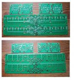
boards arrived today
not only extremely nicely designed, and in very fine quality....but also at low cost...very cool....hope its not too much to take a deep bow
Received my boards yesterday. Look great.
Thanks Georg,
Rush
Where did you read it was recommended ? It's just an exercize in simplification (and it's not even that)...Sorry Juma, I missed one point: why should be reccomended to avoid trimming pots for the JFets?....
With 15V rails and 0.6A bias am I still best of using 0R33 Rs?...
The lower the Rs, the higher the gm (yfs) of the output stage. OTOH, the lower the Rs, the higher the need for better matching of MOSFETs. Feel free to experiment and decide for yourself what you like better.
Where did you read it was recommended ? It's just an exercize in simplification (and it's not even that)...
Quoted on post #451: "....and with carefully chosen JFETs' drain resistors we can avoid trimming pots."
Maybe reccommended was too strong.... well, at least suggested as a possible option.
Thank you anyway.
Quoted on post #451: ...
Actually, post #451 quotes my answer (post #328) to "The Space Egg Corp" in his pursue of simplest working F5 schematic. It's not a clever thing to do, nor a recommendation/suggestion, but only an answer to inquisitive fellow member.
Whoever finds this idea interesting should be fully aware of what's he doing. Otherwise, please don't follow that road.
Last edited:
Then I'm in troubleWhoever finds this idea interesting should be fully aware of what's he doing.
I simply found the idea of biasing to 0.6A to limit thermal excursions very elegant and convenient.
Since Vgs @ 0.6A for these FETs is virtually the same at any temperature it will also be more reliable not to match the devices at operating temperature
I will be using pots for biasing - I'm not a suicidal minimalist
- Status
- This old topic is closed. If you want to reopen this topic, contact a moderator using the "Report Post" button.
- Home
- Amplifiers
- Pass Labs
- F5 with 2SK2013/2SJ313