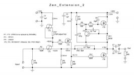
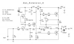
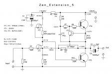
I have put together this draft schematics because of two reasons.
First, in Zen4 and Zen9, some trouble for me is caused by the serial NFB arrangement, where NFB resistor stands at the gate of the input transistor, and we must recharge the non-linear gate input capacitance through it.
Second, in Zen9, after we adjusted its square wave behavior by a small bypass cap, after applying 4 Ohms load the square wave front edge becomes very slow.
The present draft schematics distinguish by the following features:
1) Zen schematics in the output stage
2) low Ciss and fast j-fets and mosfets
3) parallel 40dB NFB arrangement
4) no capacitors in the signal path before Zen
5) high input impedance, low output impedance
The parallel NFB (resistors R10, R5) is not popular since it is connected to the low impedance point and needs a lot of current.
The source follower VT3 is used for gate level shift and making better conditions for operation of the input stage.
The input stage (VT1, VT2) should be implemented with 2SK246BL j-fets (5-6mA current), but at present I just did a trial with KP903 (CP650) 20mA current, that is actually not needed for recharging IRF610 gate capacitance.
As it could be expected, the breadboarded schematics strongly tends to be unstable and oscillates at nearly 20MHz frequency. I managed to suppresses the oscillations by adding the C6 gate-to drain capacitor, which passes definite RF power through it and becomes very hot. Therefore I made it from three 6,8pF ceramic caps in parallel.
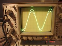
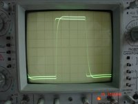
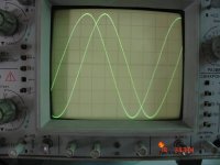
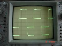
The square wave response, with 3,6 Ohms load connected, is very fast, but suffers from the front edge overshoot approx 20%, and the oscillating decay lasts for approx 2-3 μsec. I would appreciate proposals on how to fix this in more optimal way.
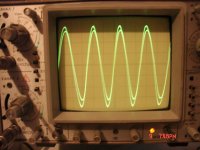
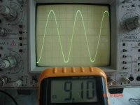
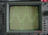
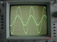
The sine wave behavior (with 3,6 Ohms load, low-signal 4V peak-to-peak) at 3MHz and 300kHz is illustrated in the shots. The bandwidth (-1dB) extends to more than 3 MHz at these conditions. There is very small visible phase shift that is difficult to estimate.
One more features that must be fixed is related with the strange effect – the output signal is not delayed against the input at 3MHz, it comes a little bit before (peak position) the input (3MHz shot). On the contrary, at 300kHz the behavior is normal, there is very minor delay of the output.
First, in Zen4 and Zen9, some trouble for me is caused by the serial NFB arrangement, where NFB resistor stands at the gate of the input transistor, and we must recharge the non-linear gate input capacitance through it.
Second, in Zen9, after we adjusted its square wave behavior by a small bypass cap, after applying 4 Ohms load the square wave front edge becomes very slow.
The present draft schematics distinguish by the following features:
1) Zen schematics in the output stage
2) low Ciss and fast j-fets and mosfets
3) parallel 40dB NFB arrangement
4) no capacitors in the signal path before Zen
5) high input impedance, low output impedance
The parallel NFB (resistors R10, R5) is not popular since it is connected to the low impedance point and needs a lot of current.
The source follower VT3 is used for gate level shift and making better conditions for operation of the input stage.
The input stage (VT1, VT2) should be implemented with 2SK246BL j-fets (5-6mA current), but at present I just did a trial with KP903 (CP650) 20mA current, that is actually not needed for recharging IRF610 gate capacitance.
As it could be expected, the breadboarded schematics strongly tends to be unstable and oscillates at nearly 20MHz frequency. I managed to suppresses the oscillations by adding the C6 gate-to drain capacitor, which passes definite RF power through it and becomes very hot. Therefore I made it from three 6,8pF ceramic caps in parallel.
The square wave response, with 3,6 Ohms load connected, is very fast, but suffers from the front edge overshoot approx 20%, and the oscillating decay lasts for approx 2-3 μsec. I would appreciate proposals on how to fix this in more optimal way.
The sine wave behavior (with 3,6 Ohms load, low-signal 4V peak-to-peak) at 3MHz and 300kHz is illustrated in the shots. The bandwidth (-1dB) extends to more than 3 MHz at these conditions. There is very small visible phase shift that is difficult to estimate.
One more features that must be fixed is related with the strange effect – the output signal is not delayed against the input at 3MHz, it comes a little bit before (peak position) the input (3MHz shot). On the contrary, at 300kHz the behavior is normal, there is very minor delay of the output.
Attachments
Last edited:
I have done some additional measurements for this schematics.
The gain is close to Ku=4,2 (1kHz sine signal measured Vout/Vin, 3,6 Ohms load). This result is surprising, I expected Ku=(R10+R5)/R5 = 3.
The output impedance is Zout = 0,16 Ohms.
The 100kHz square wave output voltage shows the front edge instability. How to suppress it in more efficient way? I consider the following variants:
- bigger cap across base-collector of VT4
- cap across collector-emitter of VT4
- 47nF cap across R10
- cap across collector-emitter of VT6
- cap across base-collector of VT5, VT6
I would appreciate any proposals.
Attachments
This is a schematics with standard parts. It is not extremely fast, but looks quite interesting as a 10W SE amp with good damping factor (more than 100 at 8 Ohms). Zout =0,075 Ohms, Gain is 23dB. Pictures show:
1) Measurement of Pmax at undistorted 1 KHz and 7,2 Ohms resistive load
2) Square wave response at 100 KHz and 7,2 Ohms load 8V p-t-p
3) Phase shift (nearly 0,16usec) at 1 MHz (input and output signals)
1) Measurement of Pmax at undistorted 1 KHz and 7,2 Ohms resistive load
2) Square wave response at 100 KHz and 7,2 Ohms load 8V p-t-p
3) Phase shift (nearly 0,16usec) at 1 MHz (input and output signals)
Attachments
Last edited:
Member
Joined 2009
Paid Member
It looks nice.
Looking at your schematic I wonder if you could configure the input as SRPP. Since the output is also SRPP it would be pretty cool to have front and back end the same !
I believe all you need to do is move the connection that R4 makes to the lower end of R3 so that it attaches to the upper end of R3.
It looks nice.
Looking at your schematic I wonder if you could configure the input as SRPP. Since the output is also SRPP it would be pretty cool to have front and back end the same !
I believe all you need to do is move the connection that R4 makes to the lower end of R3 so that it attaches to the upper end of R3.
The output is not SRPP now, it is a simple current source, but of course it could be modified towards SRPP or Aleph current source. With your proposal for the input (thanks for the good idea), we will get SRPP input. I can try this and report what happened to Zout.
I just have looked at the results of connecting of R4 to the source of VT2. Unfortunately, it seems the schematics has become less stable, I observe some traces of oscillations (scope line thickening) at the slope of sine signal.
Zout results in 79 mOhms instead of 73 mOhms before the change.
Zout results in 79 mOhms instead of 73 mOhms before the change.
I have done tests of this basic schematics with IGBT output transistors BUP314. Since IGBT have quite a large gate-to-emitter voltage (7…8 V), in this topology it is just enough for comfortable operation of VT1 without source follower. So, IRF610 is not needed, but idle current through VT1, VT2 must be few tens of mA, because of 1500pF gate capacitance of BUP314. This makes important using of high-current j-fets as CP650 here. In the schematics enclosed I used nearly 100 mA through VT1, VT2.
The scope shots show the sine and square signals at 100kHz 7,2Ohms 6V p-t-p, and also sine at 500kHz (for the phase shift estimate). The phase shift is 0,09 usec.
The scope shots show the sine and square signals at 100kHz 7,2Ohms 6V p-t-p, and also sine at 500kHz (for the phase shift estimate). The phase shift is 0,09 usec.
Attachments
- Status
- This old topic is closed. If you want to reopen this topic, contact a moderator using the "Report Post" button.
- Home
- Amplifiers
- Pass Labs
- Zen Extension