Rich - So the jfets look good. Back to the board then.
What are the voltages at the top and bottom of R9 when there is NO jfet installed at all? They should be the same and close to 20 volts.
Turn off power. With your ohmmeter, and NO jfet installed, verify that the resistors between each jfet and ground (R21 to R24) are indeed 10 ohm each.
If all is good, next verify consistency in your measurements. Solder ONE jfet and measure Q3 (all 3 pins). Remove the jfet, solder another one and repeat.
Pierre
Last edited:
Rich - Interesting. T, M, B means top, middle and bottom pin of Q3, correct? Something funny is going on. Let me chew on this for a while.
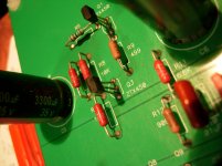
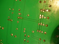
Do you think you could post a close up pictures of this area of the board (component side and solder side) ?
Pierre
Pierre - yes, definitely there is something strange going on here. I'm puzzled
")
Let's wait for Rich pictures. At least, his camera works very nicely
Best,
nAr
nAr - Yes there definitely is a problem.
Got another idea. Wondering if the board is somehow applying voltage to the gate of the jfet.
Rich - Please would you short-circuit the input to ground, and re-measure Q3 (T, M, B) with one jfet in Q6? And please would you measure the gate (middle pin) of the jfet in Q6. It should be at 0 volts. If it is not, we may have found a problem.
Pierre
nAr - Yes there definitely is a problem.
Got another idea. Wondering if the board is somehow applying voltage to the gate of the jfet.
Rich - Please would you short-circuit the input to ground, and re-measure Q3 (T, M, B) with one jfet in Q6? And please would you measure the gate (middle pin) of the jfet in Q6. It should be at 0 volts. If it is not, we may have found a problem.
Pierre
Yes, gate should be close to Ground
nAr
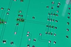
Rich - The solder joints that look shinny are good. The others... who knows? If I were you I would familiarize myself with what a good joint is supposed to look like, and some soldering 'best practices'. See for example:
Soldering - It can be done
Heat and Solder the Joints
Next, reflow and as necessary redo the joints on your board. Make sure the iron tip touches both the lead and the pad, and leave it long enough for the solder to become liquid, and really stick to the metals. Don't be afraid to heat things up! Next, verify each joint after the solder cools off. I take pliers and try to push and pull the pin to make sure it does not move. Last but not least, verify that there are no 'bridges'. That is, solder that shorts two traces together, or shorts a trace with a grounding plane.
The problem with your board could be a bridge or a bad joint.
nAr - any more suggestions? Q3 is acting funny but I can't tell if it is because of the transistor or the board... Also, grounding the input has made a drastic difference, when it shouldn't have...
Rich - The solder joints that look shinny are good. The others... who knows? If I were you I would familiarize myself with what a good joint is supposed to look like, and some soldering 'best practices'. See for example:
Soldering - It can be done
Heat and Solder the Joints
Next, reflow and as necessary redo the joints on your board. Make sure the iron tip touches both the lead and the pad, and leave it long enough for the solder to become liquid, and really stick to the metals. Don't be afraid to heat things up! Next, verify each joint after the solder cools off. I take pliers and try to push and pull the pin to make sure it does not move. Last but not least, verify that there are no 'bridges'. That is, solder that shorts two traces together, or shorts a trace with a grounding plane.
The problem with your board could be a bridge or a bad joint.
nAr - any more suggestions? Q3 is acting funny but I can't tell if it is because of the transistor or the board... Also, grounding the input has made a drastic difference, when it shouldn't have...
Hmm, R7 joint really looks like it could act funny, and be more and more "resistive" if more current is drawn by jfets ( via Q3, but also via Q1 )
I would really re-heat and add flux to all joint that doesn't look like shiny.
Especially that R8 downpin. And in doubt, re heat and add flux, to get "smooth" apparence.
For me now R8 bottom seems to me close to :
http://www.rog8811.com/soldering.htm
Model C
Joints can also become crackled when bending an already soldered component; I said it can, when joint is not done properly
Best,
nAr
Best,
nAr
Last edited:
The resistor left to the R8 (seen on top^) ; on the 2 sides, bottom solder joint of R looks bad
nAr
nAr,
cheers -just gave it the heat !
nAr,
cheers -just gave it the heat !
Heat and add some new flux. Old flux re-heated often makes bad joints.
Best,
nAr
with short across input , Q6 Gate 0 VDC
Q3, T = 17.49 VDC
M = 10.11
B = 17.36
The M (base) voltage is correct, the B (emitter) voltage should be 0.6 to 0.7V lower than the base (M), the base emitter is reverses biased, the emitter is being pulled up towards the collector, look for a short on the PCB.
Photos of my board. Note that it has not been cleaned - brown stuff is burnt flux. The resistor in parallel with R9 will be removed completely. The one in parallel with R10 stays.
Attachments
Last edited:
The M (base) voltage is correct, the B (emitter) voltage should be 0.6 to 0.7V lower than the base (M), the base emitter is reverses biased, the emitter is being pulled up towards the collector, look for a short on the PCB.
But the pad of the emitter and its trace are surrounded by ground... Instead could it be that emitter and collector have shorted inside the bjt? Or perhaps the whole ground plane is lifted up by a short elsewhere
.By the way - thanks for joining, Itsmee.
Last edited:
I get it fluid and shiny then its sets it loses its shine .... I'm using the Mundorf
M-solder and a Ersa digi 2000a @ 385 C .... I try to work on the no-more than 5 second rule ... I have trashed a lot of boards by lifting traces ...
I have now re-soldered every joint on the board
I tried a continuity test by leaving the ground connected and touch + side of components with the + probe ... nothing !
If you have a spare ZTX450, cut the legs off Q3 so as not to disturb anything, if the voltage then measures 0V on the emitter (B), the transistor was duff and the board is OK, if you still get a voltage reading, look very carefully at the trace between Q3 emitter and the JFET's drain.
- Home
- Amplifiers
- Pass Labs
- Pearl Two