Hi. Since this is the great week for me, when I'll build my long awaited (2 1/2 years!) F2, a few questions are coming up. Please return to this thread even if you answered my first question as there will probably be at least another couple or so.
So, for a start, about mounting the FETs on the heatsink. I have two options, please tell me what would be the best:
1. I found some mica locally, looks pretty good (thin but I don't know how thin, not too many scratches) and I have some Arctic Silver Ceramique
2. I bought from Mouser some Laird Technologies T-gard 5000, they don't look like those in the picture, are rectangular instead and just a bit larger than the IRFPs. I suppose they should be used without thermal compound, right?
nobody?
Nobody answers because it's pretty basic stuff - you'll be fine with either mica and white goop or with this new material (datasheet characteristics are fine) - I'd use the goop here too, it's always good to fill the small irregularities in material.
Now you have some answer.
Next guest in this thread will write about one material being better than the other, and the next one will claim the opposite, the third one will be nitpicking and revealing the mistakes of the previous two and soon you'll know the new meaning of the "being confused"

If I were you, I'd be curious to try this new material (since you already bought it) and share the experience
Lol! Thanks for your answer.
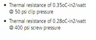
Well, just when you were writing your answer I took another look at the datasheet of the T-gard datasheet only to notice that "T-gardTM 5000 is ideal for applications that require a delta temperature across the interface of 2.0°C/watt or
higher on a TO-220 clip mounted @ 50 psi pressure." I would have thought a delta temperature of roughly 2 degrees / W (OK, it's TO-247, not 220) would not suffice for the 70W heat dissipation / 2 IRFP devices / channel of the F2...
Edit: and the mica appears to be about 0.05mm thick.
Re. the very basic question: I know it is, but this is my level of knowledge and it's not always so simple to find out what I need to know by my own. I usually use the "search" button on several forums, google it etc. before posting a question. I don't want to waste people's time, that's why I ask the questions in such a manner as to facilitate a simple answer like "Option 1." or "Option 2." I'm grateful for any help I may receive.
Thanks for your answer.Well, just when you were writing your answer I took another look at the datasheet of the T-gard datasheet only to notice that "T-gardTM 5000 is ideal for applications that require a delta temperature across the interface of 2.0°C/watt or
higher on a TO-220 clip mounted @ 50 psi pressure." I would have thought a delta temperature of roughly 2 degrees / W (OK, it's TO-247, not 220) would not suffice for the 70W heat dissipation / 2 IRFP devices / channel of the F2...
Edit: and the mica appears to be about 0.05mm thick.
Re. the very basic question: I know it is, but this is my level of knowledge and it's not always so simple to find out what I need to know by my own. I usually use the "search" button on several forums, google it etc. before posting a question. I don't want to waste people's time, that's why I ask the questions in such a manner as to facilitate a simple answer like "Option 1." or "Option 2." I'm grateful for any help I may receive.
You're right, I was calculating as if the thermal resistance would increase instead of decrease with increasing the surface! Stupid! In this case, for the ~2 square centimeters of the metallic part of the IRFPs I would get say ~0.7degrees/W which would roughly translate into a 25 degrees temperature difference between the mosfets and the heatsink. Should do, I guess...
Thanks again.
In this case, for the ~2 square centimeters of the metallic part of the IRFPs I would get say ~0.7degrees/W which would roughly translate into a 25 degrees temperature difference between the mosfets and the heatsink. Should do, I guess... Thanks again.
http://www.diyaudio.com/forums/pass-labs/37262-mica-goop.html has been and still is being discussed there.
What will you be mounting? The TO-247AC package has an isolated mounting hole, so no need to isolate the screw. Nelson is using washers to spread the force over the device, as can be seen in the pictures of the insides of the various F amplifiers.
What will you be mounting? The TO-247AC package has an isolated mounting hole, so no need to isolate the screw. Nelson is using washers to spread the force over the device, as can be seen in the pictures of the insides of the various F amplifiers.
Last edited:
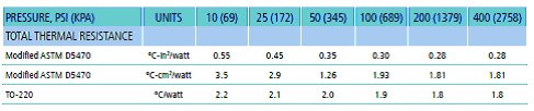
Juma, why am I wrong again? In the datasheet it says 1.26 degrees/square cm/W (see attachment), so at about 2 square cm IRFP surface this would give about half or 0.63. I rounded it up to 0.7 just to be sure. 1 square inch is > 3 times the IRFP surface and that's why the figure / square inch is much lower. If the heatsinks I am building will be efficient enough, around 0.3 C/W that is, during the hot summer days when I get a bit over 30C in my room the contact surface of the mosfet should be at 70-75 Celsius. I hope this would be acceptable.
On the other hand, there comes Rodeodave just to fulfill your predictions. Well, you didn't actually make a recommendation, Rodeodave, and I'm not confused (yet) but the thread you pointed me at (thank you) seems to suggest that mica and thermal compound make a pretty good, tried and safe combination that should give around 0.4 degrees / W - but I didn't understand on what surface, perhaps you know? Is it on a square inch? Yes, I will use washers.
Another thing in this thread that popped into my attention is the recommendation to smooth sand the surface of the transistor as its plastic border could be higher than the metal surface and thus keep it from getting into contact with the heatsink. Unfortunately, 600 or 800 sandpaper has been mentioned and the best I have found so far was only 240... Not to mention that I have to smooth the surface of the diy heatsink (not such a good idea btw, but now it's already 70% done) because drilling the holes for the mounting screws resulted in an elevated rim around each hole.
I e-mailed Laird Tech. asking if their product should be used in conjunction with a thermal compound or not and I got the following answer:
On the other hand, there comes Rodeodave just to fulfill your predictions.
Well, you didn't actually make a recommendation, Rodeodave, and I'm not confused (yet) but the thread you pointed me at (thank you) seems to suggest that mica and thermal compound make a pretty good, tried and safe combination that should give around 0.4 degrees / W - but I didn't understand on what surface, perhaps you know? Is it on a square inch? Yes, I will use washers. Another thing in this thread that popped into my attention is the recommendation to smooth sand the surface of the transistor as its plastic border could be higher than the metal surface and thus keep it from getting into contact with the heatsink. Unfortunately, 600 or 800 sandpaper has been mentioned and the best I have found so far was only 240... Not to mention that I have to smooth the surface of the diy heatsink (not such a good idea btw, but now it's already 70% done) because drilling the holes for the mounting screws resulted in an elevated rim around each hole.
I e-mailed Laird Tech. asking if their product should be used in conjunction with a thermal compound or not and I got the following answer:
Thought about sharing it, perhaps could be useful to others as well.Basically T-gard 5000 will fill micro undulations on the surface of the top/bottom heat transfer mediums, but as T-gard 5000
is only 0,005" = 0,127mm thick, the efficiency of this process is limited.
T-gards are actually just Thermal Interface Insulator materials.
Thermal greases will not decrease thermal performance and could be used to fill rougher top/bottom surfaces.
Attachments
Funny, I got another e-mail from Laird:
Oh, and the mica I got is 0.01mm (0.004'') thick, might be a bit too much.
With cc to my previous respondent, who probably has not been very happythe material needs no other compounds and will take up the regularities of the transistor and heatsink providing they have good mating surfaces.
Best Regards,
Keith McDonald
Global Sales Director : Thermal Products
Laird Technologies
Oh, and the mica I got is 0.01mm (0.004'') thick, might be a bit too much.
this is the last obstacle, please help me jump straight onto the finnish line!
The amp is almost finished. I have decided to use mica and compound, I managed to find some suitable (thin) mica locally but, unfortunately, I still have a problem regarding the compound application. Please tell me what is the correct way to do it.
I'm using as I said before Arctic Silver Ceramique. I have tried to apply the method described for computer procesors on the Arctic Silver site, i.e. applying the compound on one surface (transistor and heatsink surfaces, in my case), then removing it (which should have theoretically resulted in a slightly dull surface due to the compound remaining in the microscopic valleys of the surface) and applying a blob of compound on the opposite surface (both surfaces of the mica washer, in my case) and mounting them all together with a screw. Problem is that after applying compound on the transistors, it either gets cleaned 99.999% completely, or (if I apply less pressure when attempting removal) the remaining layer is very uneven. I have tested this by putting the mica washer on top and in spite of me sliding the two surfaces against each other a bit and pressing them together I could see through the mica washer that only 40-50% of the surface was really in contact through the compound.
What is the correct application method in my case? How much compound should remain on a surface after the removal manoeuvers?
Please help me put this F2 under the Christmas tree!
Thank you!
PS I hope I was coherent enough, I'm extremely tired after working at the amplifier all night long and many other very tiring previous days and nights (I've built myself the enclosure and the heatsinks too).
DQ, I dont apply mica to both sides of the mica, but I dont see anything wrong with it, other than it might look messy.
When I use either thermal grease, or artic silver, I put a small dap of it in the center of where the MOSFET will go, or a little under the mounting hole. I then put the mica or silicon pads on top of it, and rub it around a bit, centering it to get the hole in the mica to match with the bolt hole. After tightening, if it's missing a spot, or excess comes out the side, I dont worry about it. In the later I clean it up a little.
Then I test for shorts of the fet by testing for continuity between MOSFET metal tab in front and chassis. If there is no continuity, fire it up.
... I dont apply mica to both sides of the mica....
How do you achieve that ?

Sorry, I couldn't resist
How do you achieve that ?
Sorry, I couldn't resist
Had you been just a little clever, you'd know
Simple really, only apply a mica washer to one side of the mica washer
Magura
Many many thanks to you guys for the very quick answer!! You are a treasure - several treasures, actually I don't know if I worry too much, it's just I didn't know the correct technique and I believe this particular building step ought to be done right. After the huge amount of work I have done building these sinks I'd rather not ruin the heat transfer at this point.
The "mica on both sides of the mica" reminds me of my high school years. The biology teacher asked us to "make observations" on some zoological relics such as the shell that was allotted to me. I wrote that it has two sides and I underlined that they are opposite to each other
I don't know if I worry too much, it's just I didn't know the correct technique and I believe this particular building step ought to be done right. After the huge amount of work I have done building these sinks I'd rather not ruin the heat transfer at this point.The "mica on both sides of the mica" reminds me of my high school years. The biology teacher asked us to "make observations" on some zoological relics such as the shell that was allotted to me. I wrote that it has two sides and I underlined that they are opposite to each other
Are you serious? I really think it's somehow funny how the only thing you're worried about is mica and goop. ;-)
The way I usually approach this step is applying some goop (with a toothpick) to the area on the heatsink, apply some goop to the transistor, attach mica to it and place the whole thing on the heatsink. Tighten screw, bring to the boil, tighten screw again, relax.
The way I usually approach this step is applying some goop (with a toothpick) to the area on the heatsink, apply some goop to the transistor, attach mica to it and place the whole thing on the heatsink. Tighten screw, bring to the boil, tighten screw again, relax.
Actually it's not the only thing that worried me during the whole building process I have mounted the mosfets yesterday evening, thanks anyway.
The next thing that worries me, if you really wanna know, is that my diy sinks are rather thin, albeit big in all the other regards. This is just being addressed in a parallel thread, but it was another builder posting. Hope mine will work well. Since the PSU is done and tested well, tonight after soldering the wires to / from connectors and between the pcbs I will find out. Finger crossed
I have mounted the mosfets yesterday evening, thanks anyway.The next thing that worries me, if you really wanna know, is that my diy sinks are rather thin, albeit big in all the other regards. This is just being addressed in a parallel thread, but it was another builder posting. Hope mine will work well. Since the PSU is done and tested well, tonight after soldering the wires to / from connectors and between the pcbs I will find out. Finger crossed
- Status
- This old topic is closed. If you want to reopen this topic, contact a moderator using the "Report Post" button.
- Home
- Amplifiers
- Pass Labs
- Building the F2 - teach the newbie please! (one question at a time)