Nice.
Checkout
http://www.borbelyaudio.com/adobe/ae699bor.pdf
See Figure 15c and table 3. You can lower your THD even further, and reduce the DC offsets at the output.
However watch out for your XO impedances, they can introduce more THD than what you would want. Also, if you need higher XO frequencies, you may want to think about cascode to reduce input capacitance.
Leo
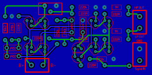
My Shot at a PCB`
Whipped this up. Was thinking of putting all resistors in a ladder formation and the 2sk170's side by side in pairs then in a ladder as well. Might try that and see how it goes but here is my first try.
This is optimized for space and for Dale 1/4W resistors or smaller. Larger resistors would work but more than 1/2W might be trouble. I imagine PRP would be fine.
This is double sided. Single sided is a pain with the power lines needing to be so close.
---What I am not sure about here is whether the caps and resistors are going to a ground or to B-...?? I see that the sign for B- on the source of the 2sK's is the same as what I have interpreted as a ground on the caps/resistors.
Uriah
Attachments
Last edited:
Whipped this up. Was thinking of putting all resistors in a ladder formation and the 2sk170's side by side in pairs then in a ladder as well. Might try that and see how it goes but here is my first try.
This is optimized for space and for Dale 1/4W resistors or smaller. Larger resistors would work but more than 1/2W might be trouble. I imagine PRP would be fine.
This is double sided. Single sided is a pain with the power lines needing to be so close.
---What I am not sure about here is whether the caps and resistors are going to a ground or to B-...?? I see that the sign for B- on the source of the 2sK's is the same as what I have interpreted as a ground on the caps/resistors.
Uriah
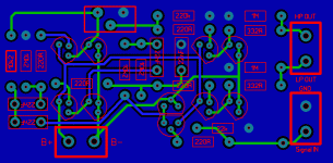
Uriah,
My apologies for the not-so-clearly labeled schematic. This attachment should take care of that. Frankly, I didn't anticipate anyone posting a PCB layout this soon. It hasn't even been breadboarded yet

I'm having a little trouble following your board layout. I don't see the connection from the input and output buffers (Q1, Q2, Q5, Q6, Q9 and Q10) to B-. I also do not see a signal connection from the input buffer to the HP and LP sections.
Jacques
Attachments
Uriah,
Frankly, I didn't anticipate anyone posting a PCB layout this soon. It hasn't even been breadboarded yet
Jacques
I think there is a lot of interest Jacques, and don't be surprised if someone else already has!!
I'm certainly thinking about starting to work on a verro board layout The Spice sims look very promising, and I'm rather intrigued by your solution to the stopband response problem , though the sim certainly shows it does the Trick!Tony.
the 2pole (-12dB/octave) has Q=0.5 to create the L-R function.This a 2 pole (12dB/oct) LR filter at 700 Hz. It should be fairly straightforward to implement 24dB/oct.
A 4pole using two cascaded sections of 2pole requires both sections with Q=sqrt(2). two cascaded Q=0.7071 gives an overall Q=0.5
This is the normal Butterworth roll off and needs the feedback components doubled up to create R & 2R in both the HP sections and C & 2C in the LP sections.
go to Linkwitz site.Could you post the formulae for the RC values for those of us that are challenged? Additionly I assume this is a unity gain. If so can the gain be increased.
If you use gain stages then the gain controls the Q. It becomes a very different design if you adopt other than unity gain.
You can use ECV Sallen Key or MFB as your gain filter stages.
Uriah,
I also do not see a signal connection from the input buffer to the HP and LP sections.
Jacques
The other missing traces I dont know how I missed them last night. I had removed them and moved the power input and signal input around the board. Must have got caught up with family stuff and thought I fixed them. I think I found a good spot to get the signal from initial 2sk pair to the junction of 22nF and 10k2.
I think I still want to redo the entire layout in that ladder style.
So what kind of capacitors were you thinking of using? Are they regular Wima Box style or are these the big audio caps like Nelson had on the original B1?
Uriah
Last edited:
Jacques
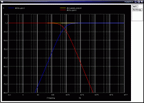
I wonder if it won't be better to do the same on with the hi-pass section as you do with the low-pass section. (Please excuse the different labeling)
The green plot is at the input of R4, the blue plot is at the output of J3.
Johnny
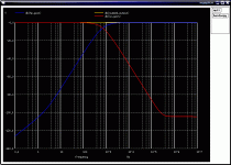
I wonder if it won't be better to do the same on with the hi-pass section as you do with the low-pass section. (Please excuse the different labeling)
The green plot is at the input of R4, the blue plot is at the output of J3.
Johnny
Attachments
Last edited:
Hi all, this looks like just what I need as well. Could you post the formulae for the RC values for those of us that are challenged?
For the 2 pole LR use:
R = 1 / (2 * PI * f * C)
Andrew,
Using SIP... I found this one 310-13-120-41-001000 20P IC Socket Mouser 2.32 ea.
Hope they will do the job. It will take a 15-25mil lead.
I was thinking to make the board a lot bigger and single sided so people can etch it themselves. I can put room at each cap position for caps with 5mm, 7.5mm, 10mm and 15mm pin spacing. I am making the resistors bigger to so they can accomodate resistors up to 12mm long plus leads. I cant stand boards that only make room for 5-6mm resistors. Since I am making the components bigger I get to have a larger board, which does have its drawbacks, but it will probably allow me to do single sided. So I will work on it over the next few days.
If everyone thinks just WIMA box caps are fine here then I think I have all the info I need, but I wonder if people are going to want to use big caps like Axon, Mundorf, etc..
Uriah
Last edited:
So what kind of capacitors were you thinking of using? Are they regular Wima Box style or are these the big audio caps like Nelson had on the original B1?
Uriah
I'd like to avoid making specific part recommendations beyond good quality film types with tight tolerance.
I will probably establish a baseline for evaluating more exotic parts with the Panasonic 1% film caps available from Digi-Key.
Jacques
I wonder if it won't be better to do the same on with the hi-pass section as you do with the low-pass section. (Please excuse the different labeling)
The green plot is at the input of R4, the blue plot is at the output of J3.
Johnny
loading C2 with 10k2//22k completely upsets the filter.
The buffer MUST show near infinity input impedance for the filter to work properly.
Similarly the input buffer MUST present a near zero source impedance to the filter for it to work as expected.
Johhny,
There's no advantage to it that I can see. Also, AndrewT's advice is spot on. In your schematic, you need to remove U1/U2 and R6/R13.
The rationale for providing a separate buffer for the feedback cap is that at high frequencies, the input signal is shunted through the feedback cap and appears (attenuated) across the output impedance of the buffer, wrecking the stopband attenuation. That path doesn't exist in the high pass section.
You can refer to this article from EDN for additional information.
- Status
- This old topic is closed. If you want to reopen this topic, contact a moderator using the "Report Post" button.
- Home
- Amplifiers
- Pass Labs
- B1 Active Crossover