Hi All
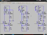
I have ready now the pcb for the alfet amp who is based on the pass labs except the power stage.
The output resistor is tegehter wilh a coil who is not visible on the pcb,
here the pictures
I have ready now the pcb for the alfet amp who is based on the pass labs except the power stage.
The output resistor is tegehter wilh a coil who is not visible on the pcb,
here the pictures
An externally hosted image should be here but it was not working when we last tested it.
An externally hosted image should be here but it was not working when we last tested it.
An externally hosted image should be here but it was not working when we last tested it.
Hi All
I have ready now the pcb for the alfet amp who is based on the pass labs except the power stage.
...
What Pass Labs design it might be?
What did you use for output devices ?
Last edited:
Hi
I have based it on the pass laps ALEPH 1.2
I only used the inputstage of it.
the output transistors are the 2sj 162 and the 2sk1058.
the drivers are the irf 610 and the irf 9210 in constant current mode, with correction circuit to keep it constant with high output voltages, (stability).
the output is class a to ab depending of output power, I have 10 watt class a after that it goes ab so I spare some energie") the original pass labs uses a constant current (also with correction for stability) in the output stage of some amps, it uses therefore much energie.
the original pass labs uses a constant current (also with correction for stability) in the output stage of some amps, it uses therefore much energie.
I have based it on the pass laps ALEPH 1.2
I only used the inputstage of it.
the output transistors are the 2sj 162 and the 2sk1058.
the drivers are the irf 610 and the irf 9210 in constant current mode, with correction circuit to keep it constant with high output voltages, (stability).
the output is class a to ab depending of output power, I have 10 watt class a after that it goes ab so I spare some energie
the original pass labs uses a constant current (also with correction for stability) in the output stage of some amps, it uses therefore much energie.My circuit is not already adjusted for output bias. Output idle current will be determined by R7.
My idea in post 1904 is a dud...
Anyways this is not our thread, maybe we should go in private or make our own thread.
- keantoken
Oke we give this thread new live, I like the idea of the nmosfets with a aleph idea.
I have tryed it, but is presume that that driver mosfet has the impedance factor and drive power? because mosfets has a lot of capacity, although the way we do it now it is less important.
Last edited:
Let me copy my important post from the other thread.
Here are some examples.
The first is the simplest. The compensation resistor, R4, is integrated into the bootstrap. Because the current through this resistor will mirror the current through R2, it's voltage drop will also be that of R2, to the Vgs of each output will be balanced and the outputs will equally share the load.
In the second, the CCS is still used, but it will have to have twice the VAS current because it must now also provide the current through R9.
In the third example, there is a cap in series with the 120R resistor, to block DC so the CCS current can be decreased. Overall, the first scheme should appeal for it's simplicity, and the second scheme should appeal to those who dislike caps. I don't know why anyone would use the third scheme, but it's an option.
Also, the .22R resistors you have placed on the drains of the upper outputs are not doing anything helpful. They should be placed at the sources instead, like in my schematic.
- keantoken
Attachments
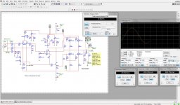
I have tryed i, I have used your middle solution on picture without a cap to keep current high for driving mosfet gate.
I have discover that simulation of that quasi thing is not so easy, for multisim it is a strange circuit, however I have nice specs, but fake the load, so I am not shure, with 8 ohm it collaps what is strange for a mosfet,.
I have discover that simulation of that quasi thing is not so easy, for multisim it is a strange circuit, however I have nice specs, but fake the load, so I am not shure, with 8 ohm it collaps what is strange for a mosfet,.
Attachments
Your gate stoppers for the lower MOSFETs are connected incorrectly.
Also, C4 should be connected to the drain of Q1, unless there is a specific reason you're doing this.
D7 and D4 will cause large problems, if these conduct the output will clip to the rails. They do not protect anything I'm aware of, and their junction capacitance may worsen amp performance.
- keantoken
- Status
- This old topic is closed. If you want to reopen this topic, contact a moderator using the "Report Post" button.
- Home
- Amplifiers
- Pass Labs
- pass labs basis allfet amp.