I have just re-read your post. Do I read you have an output DC offset of 130mV?
If this is the case then perhaps this is too high. I asked on this thread what level of DC offset would be too high. The answer was anything over 20mV and in fact my amp is reading only 1 or 2mV at present. See here: http://www.diyaudio.com/forums/pass-labs/150653-burning-amplifier-ba-2-a-75.html
Best wishes,
Chris
Dear Chris hi,
This is the measurement on right channel left channel measures approximately at 160mV.
I do not have any other turns to trim either on P102 or P201 (front end).
Any good ideas ???
deep 6?
Hello.
I'm in the process of making the ba3 with the deep 6 ...
boards I have is 4xba-co v2.0 and 4xBA-CB (same as pic above)
So after reading and reading the confusion is bigger than ever
How do I connect the boards? do I use two bias boards? or do I series connect the BA-CO to the other BA-CO only using 1 bias board?
Any help would be apreciated.
diynewbi
stig
Hi
This is my interpretation of the wiring of the boards. Have I drawn it right or have I got it backwards?
An externally hosted image should be here but it was not working when we last tested it.
Even though the picture isn’t very good it’s sometimes easier to make a simple drawing than explain it in words.
Kind regards
/Forsman
Hello.
I'm in the process of making the ba3 with the deep 6 ...
boards I have is 4xba-co v2.0 and 4xBA-CB (same as pic above)
So after reading and reading the confusion is bigger than ever
How do I connect the boards? do I use two bias boards? or do I series connect the BA-CO to the other BA-CO only using 1 bias board?
Any help would be apreciated.
diynewbi
stig
do I series connect the BA-CO to the other BA-CO only using 1 bias board?
That would be correct.
Lay out the two output boards with the short sides side by side, maintain the 40mm spacing for the fets between the boards, then place the bias board on top and between the two output boards, the fixing and connection holes for the bias board will line up with the holes in the output boards, you will then have short vertical connections between the boards.
Dear Chris hi,
This is the measurement on right channel left channel measures approximately at 160mV.
I do not have any other turns to trim either on P102 or P201 (front end).
Any good ideas ???
Itsmee is correct. Use P102 to reduce the DC offset.
Adjusting DC offset on the front end won't alter the power board output because of the 10uF capacitor which soaks up any DC (you still need to reduce DC offset on the front end though).
You should be able to get the DC offset from the loudspeaker outputs to a very low figure. I have just checked mine whilst putting in a voltage reg and they are on the left channel about 0.0V and on the right 5mV.
I have also checked the mV readings across the 1ohm resistors on the power boards. They were between 378mV and 388mV.
Chris
Dear all,
Two problems on output stage.
Bias current on left channel
I have measured all bias resistors on both channels and they are very close to given reference values.
Left channel example of that values (the problematic one (40mv bracket) in comparison to right channel (10mv bracket)).
Left channel
IRFP9240
1ohm- 149,4ohm
1ohm - 150,6ohm
1,1ohm- 149,4ohm
1,1ohm -149,8ohm
1.1ohm -149,6ohm
Right channel
IRFP9240
1,1ohm - 149,9ohm
1,1ohm -150ohm
1,1ohm -150.2ohm
1,1ohm -150ohm
1,1ohm -150ohm
High Output stage DC-offset value on both left and right channel
Left channel 160mV and right channel 130mV
Can someone with more experience advice on how we can resolve these problems?
Thanks for all the help and support
Dear all,
Two problems on output stage.
Bias current on left channel
I have measured all bias resistors on both channels and they are very close to given reference values.
Left channel example of that values (the problematic one (40mv bracket) in comparison to right channel (10mv bracket)).
Left channel
IRFP9240
1ohm- 149,4ohm
1ohm - 150,6ohm
1,1ohm- 149,4ohm
1,1ohm -149,8ohm
1.1ohm -149,6ohm
Right channel
IRFP9240
1,1ohm - 149,9ohm
1,1ohm -150ohm
1,1ohm -150.2ohm
1,1ohm -150ohm
1,1ohm -150ohm
High Output stage DC-offset value on both left and right channel
Left channel 160mV and right channel 130mV
Can someone with more experience advice on how we can resolve these problems?
Thanks for all the help and support
What are these figures? 1.1ohm-149.9ohm. Should this read 1.1ohm-149mV reading across the resistor?
What are these figures? 1.1ohm-149.9ohm. Should this read 1.1ohm-149mV reading across the resistor?
No dear Chris they are the values that i am geting after measuring the bias resistors on the output stage.
Ref valus are 1 ohm and 150 ohm.
Zen Mod advice was to check for posible differences
I told you about possible differences between source resistors (in value )
those 150 ohms resistors aren't "bias resistors" in any meaning ; they're gate stoppers , intended for preventing oscillations and somewhat for shaping frequency response of mosfets
do your homework - read all Papa's papers , if not for your own pleasure - then from respect for his sharing ; papers are written to be read .
adjust DC offset on output with P2 on output stage
do your homework - read all Papa's papers , if not for your own pleasure - then from respect for his sharing ; papers are written to be read .
adjust DC offset on output with P2 on output stage
He's absolutely right.
I told you about possible differences between source resistors (in value )
those 150 ohms resistors aren't "bias resistors" in any meaning ; they're gate stoppers , intended for preventing oscillations and somewhat for shaping frequency response of mosfets
do your homework - read all Papa's papers , if not for your own pleasure - then from respect for his sharing ; papers are written to be read .
adjust DC offset on output with P2 on output stage
Dear Zen Mod,
Appreciating your "refer to "on fundamental references.
I myself have studied the manual very thoroughly.
If you have the time to read with more attention you will see that i have pointed out on post 901 on this thread that I do not have any other turns to trim on P102.
Additionally
When you suggested to check the source resistors for possible variances i thought that measuring also the 150 ohm resistors is a good idea in terms of providing a more complete picture.
If this measurement is irrelevant to the problem i do apologize.
Finally please do not make any assumptions that lead to falls conclusions.
In any case thanks for all your help and support.
.....
Finally please do not make any assumptions that lead to falls conclusions.
........
nobody is perfect , except me ....... and (just ) maybe Papa .....

anyway - fact is that you mention gate resistors as possible culprit in individual biasing of mosfets ; that can lead to confusion any other greenhorn reading these posts in future ....
turn off amplifier ;
turn pot P2 approx. to middle position ;
if offset is positive - solder 220K resistor across R25
if offset is negative - solder 220K resistor across R26
turn on , set offset with P2
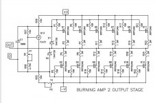
setting offset - referring to this attached schematic :
(FE doesn't have anything with output offset )
Attachments
Last edited:
nobody is perfect , except me ....... and (just ) maybe Papa .....
anyway - fact is that you mention gate resistors as possible culprit in individual biasing of mosfets ; that can lead to confusion any other greenhorn reading these posts in future ....
turn off amplifier ;
turn pot P2 approx. to middle position ;
if offset is positive - solder 220K resistor across R25
if offset is negative - solder 220K resistor across R26
turn on , set offset with P2
setting offset - referring to this attached schematic :
(FE doesn't have anything with output offset )
Is this to compensate for possibly unusual difference in N vs P parts? Reason for checking offset polarity is to identify which side is in need of compensation.
Any idea how large?
high impedance load = smaller cap
lower load impedance = bigger cap
Measure the source resistors to see if the fets are sharing current equally or close. If you followed the schematic exactly, they should be the 1R 3W resistors.
Dear Buzzforb hi,
Olready did that
Post #907
I do not see significant value differences on the source resistors .
Left channel
IRFP9240 (40mV bracket)
1ohm
1ohm
1,1ohm
1,1ohm
1.1ohm
Right channel (10mV bracket)
IRFP9240
1,1ohm
1,1ohm
1,1ohm
1,1ohm
1,1ohm
Thanks
- Home
- Amplifiers
- Pass Labs
- Burning Amplifier BA-2