Just finished th F5 today. Initial setup looked good, both sides were about .59v for R11 & 12. Both channels are hot to the touch and can hold my hand to them for 5 seconds or more without any problem. The temp ramped up for over an hour.
However, I have -8.5v DC on the output of 1 channel and .5v on the output of the other channel.
I shut it off and checked the wiring and it looked ok.
There is 23v+- from the power supply. Before adjusting the voltage is was showing 25.1v.
I might have a short somewhere. Not sure where though.
The + and - on one channel output are continuous, the other is not. I took the board off the heat sink and the shorted output went away. Could it be a FET shorted to the heat sink? I didn't see any shards poking the FETs.
Sounds like I have bad FETs. Can anyone help me verify? Any other ideas where to check?
LEDs light up so at least I have an expensive, heavy and hot night light!
Thanks in advance!
Vince
Vince,
Before I hook up the Power supply and signal grounds, I do a continuity test between the metal tabs on the FETs and the heatsink. A shard going through the pad will BEEP every time...
So I guess I would try to lift grounds first.
If it doesn't short out and blow a fuse or smoke, with those kind of voltages, I would think a resistor might be out of place somewhere, or the pot's are way off, but they would not both read that voltage if that were so. At that voltage, they should be pulling plenty of current.
Another stunt I have done is get the postive or OUT binding post touching the chassis. That will cause some problems.
I think your close. These things happen to ensure that we stare troubleshooting in the eye.
Thanks Tea. I will check the tabs...these are accessible from the front of the Fet correct? They look like this |) o (| The divit shows some metal. This is what you are referring to?
Funny thing is, the gold anodizing on my heat sinks doesn't conduct well. I am using a pad between the sink and the FET.
I'll keep looking...it's always the last thing you find!
Thx,
V~
Funny thing is, the gold anodizing on my heat sinks doesn't conduct well. I am using a pad between the sink and the FET.
I'll keep looking...it's always the last thing you find!
Thx,
V~
with grounds lifted from ground bus, and boards attached to sink, does it still short between tab and heatsink.
I've had to file and sand (with 1200 grit) the heatsinks spots and tap hole to get a perfect fit, bit I never attach to heatsink first, it would keep bending to a minimum on a FET I suppose.
Often movign the heatsink pad around the whole is needed to keep it from shorting, if it's not a metal shard.
I assume you shorted inputs.
vdi_nenna said:Yes, used the Cviller F5 update manual. Followed it carefully. I did not install FETs while on the heat sink. Don't know how critical this is. Is it?
Thx,
Vince
If you are using the Zetex transistors, make sure that you have the P and N devices correctly oriented (not as shown on the silkscreen).
Examine the board with a magnifying glass -- I fixed one board for someone and there was a tiny ball of solder shorting out TO-92 transistor leads. In another the boards were finicky about soldering (I like tinned boards, not plated boards.)
A burr on the back of a TO-247 transistor, or on a mounting hole with a burr, or even some drilling detritus will cause a "bad-hair day".
vdi_nenna said:
However, I have -8.5v DC on the output of 1 channel ...
With my latest F5, I had a similar problem, which was due to a collapse of balancing between the upper (positive) side and lower (negative) side. I did check all passive components and found they were all right. In addition, I did check whether the drains of the mosfets were shorted to the heat sinks, but they were all found as well insulated. My problem was finally found as having come from the input jfets damaged due to over-temperature of soldering iron.
Hope you will find a solution soon . . .
with grounds lifted from ground bus, and boards attached to sink, does it still short between tab and heatsink.
I will check this tonight. Also, I have better sink pads in storage. The current pads are flimsy at best. I have the...what are they called...oxide ones in storage. They are thick.
What I don't understand is how the hex bolt could make contact with the case. There is a gap of plastic seperating the metal part on the back of the FETs. I do have shoulders
If you are using the Zetex transistors, make sure that you have the P and N devices correctly oriented (not as shown on the silkscreen).
I'll triple check the Zetex trans. From memory, I can say the Zetex cbe are reversed from the BC trans.
I believe I have 2 seperate issues, maybe multiple ones for each channel. Can't rule that out.
Guessing since voltages are ok (not great) and the fuse isn't blowing, that I'm partically there? Could be worse, right?
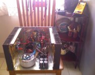
Here's a pic of testing. Using 2 digital and one analog. all the test equipment I have, although I can grab a o'scope from storage, but not sure how to use it.
Attachments

vdi_nenna said:
I'll triple check the Zetex trans. From memory, I can say the Zetex cbe are reversed from the BC trans.
I believe I have 2 seperate issues, maybe multiple ones for each channel. Can't rule that out.
Guessing since voltages are ok (not great) and the fuse isn't blowing, that I'm partically there? Could be worse, right?
Here's a pic of testing. Using 2 digital and one analog. all the test equipment I have, although I can grab a o'scope from storage, but not sure how to use it.
Yeah, you're right the zetex should be placed with the curved side reversed from the footprint on the boards. You can also pull them out when you get desperate - they are not essential for adjusting the bias.
Have you tried comparing the working channel to the bad one - any differences? What about the jfets - have they been swapped n/p channel?

Regarding the adjustments, the purpose is not only to get the current through R12 and R11 to be approx 1.3A (0.59V/0.47ohm), but also to adjust the DC output. You could try to turn down P2 (low resistance) until you get ~0V on the output and then check what your voltages are over R11 and R12.
Have you tried comparing the working channel to the bad one
I think I have 2 bad channels. Different issues in each.
The one channel I'm sure is shorted somewhere, possiblly the FETs or the input. I remember the input of 1 RCA being real tough to insert the male RCA. It popped and then it went in, so I have to investigate.
The other channel, I get -8.5v at the output.
Both channels warm up gradually as if they were working fine.
Do you know if connecting the F5 PCBs GND OUTs to the output jack require additional grounding to star or power ground?
I have the PS boards grounded to a single point, then to earth ground. The audio PCB has a GND out and it goes to the speaker jack on the chassis only. Should it also go to star or earth ground?
Thanks,
Vince
vdi_nenna said:
I think I have 2 bad channels. Different issues in each.
The one channel I'm sure is shorted somewhere, possiblly the FETs or the input. I remember the input of 1 RCA being real tough to insert the male RCA. It popped and then it went in, so I have to investigate.
The other channel, I get -8.5v at the output.
Both channels warm up gradually as if they were working fine.
Do you know if connecting the F5 PCBs GND OUTs to the output jack require additional grounding to star or power ground?
I have the PS boards grounded to a single point, then to earth ground. The audio PCB has a GND out and it goes to the speaker jack on the chassis only. Should it also go to star or earth ground?
Thanks,
Vince
You must have a gnd connection between the boards and the psu, input and output. The topology (what kind of start) you choose will affect only the noise level.
You could try to edit my picture:
http://viller.eu/audio/2009jan_gbf5/P1070474_wiring1.jpg
and show your wiring scheme.

Tea-bag and All,
With the left channel boards attached with the ground bus intact, there's continuity...it's shorts. Lifting the ground form the bus there is no continuity...no short.
I also found that the input on the left or right are not shorted, but the positive speaker out on the left is shorted!! This is with the board off the heat sink and ground attached.
I found the aluminum oxide pads. I'll clean up the goop and feel around for burs in the heatsinks.
Can I assume the FETs are burned at this point?
Thanks,
Vince
- Status
- This old topic is closed. If you want to reopen this topic, contact a moderator using the "Report Post" button.
- Home
- Amplifiers
- Pass Labs
- Pass F5 Help Needed