Hi babo
See this post: http://www.diyaudio.com/forums/showthread.php?postid=1572606#post1572606
I am") to see other peoples interested finally...
to see other peoples interested finally...
See this post: http://www.diyaudio.com/forums/showthread.php?postid=1572606#post1572606
I am
to see other peoples interested finally...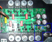
Hi Fab,
Your project and results are very interesting
And, thanks for the info about Class XD and Displacer.
BTW, in connection to Fig.5, the additional SE bias, I'm reading Aleph 0s output and its SE CCS bias . . . (for me to try for my F4 hopefully soon) . . . And, I'm wondering where the "ISD" is going to? Do you (or anyone) know about this?
Fig 5 doesn't have an Isd, but referring to that figure, at idle the
current which passes through the constant current source comes from
the current going from the positive supply through the N channel
output, through the current source to the negative supply.
For positive output current, the current source continues to get its
current through the positive output transistor. For negative output
current, it will start to also draw from the load, and at some
sufficiently high negative output current, it will draw entirely from
the load as the positive output shuts off.
Papa,
Many say that one picture tells more than 1000words. For me, however, your words are easier than the picture. Thanks for the so kind explanation.
I'm going to try to modify (improve?) my F4 with two things:
Many say that one picture tells more than 1000words. For me, however, your words are easier than the picture. Thanks for the so kind explanation.
I'm going to try to modify (improve?) my F4 with two things:
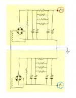
- Power supply (change in small detail as shown in the attached sketch)
- Installation of the additional SE bias ccs
[/list=1]
Thanks to your explanation, I would keep my confidence with the SE ccs which to be arranged between the output and the negative supply, and just try to decide what type of ccs.
Hoping I could do these soon . . .
Attachments
Choosing bias - some questions. I have searched, googled, and read lot's of stuff - but so much info on the net (even on this site) is contradictory.
If you can keep the MOSFETs cool, it seems like the current could be cranked way up and still be within the SOA of the outputs, the source resistors may need to be beefed up. Is this a correct statement? where is the limit? Is that limit a point that destruction occurs or does sound quality start to suffer beyond some point?
I built an F5 as designed and an F5 with 2 pairs of outputs. I biased them both higher and lower with forced air cooling for testing. I used the Fairchild devices.
I did this experiment primarily because I am driving speakers which are 2 ohms across some of their operating range and would like to stay in class A as long as possible - I also want to figure out the relationship between bias and sound quality at low output levels. For this experiment heat and current draw are not concerns.
I biased the 2 pair F5 at a slightly higher 1.5 amps per device for a total of 6 amps - it will drive my speakers almost to the voltage limits of the power supply in class A. The mounting tab of the mosfets stay around 52c
to my ears both amplifiers sounded best with the recommended bias current or more. I have a hard time removing volume from the equation though.
I understand that lowering the bias seems to lower sound quality even while still in class A mode - I am not sure if this is true, but seems to be the case, or maybe it is some kind of placebo effect (it's not getting super hot - it must not sound good!)
Originally I was thinking that if I only needed a few watts (say for active tweeter operation) I could lower the bias to lower heat and consumption, but keep the amp in class A operation for the few watts I need - it seems like there is a penalty for that and I would be better to lower the rail voltage to get my desired output for an intended impedance. Is this the case?
..Hoping I could do these soon . . .
I was wondering the other day how the Babo is doing?...been very quiet for a long while. Good to see you back!

If you can keep the MOSFETs
cool, it seems like the current could be cranked way up
and still be within the SOA of the outputs, the source
resistors may need to be beefed up. Is this a correct
statement? where is the limit?
No, with higher current, the Source resistors can remain the
same, or if cooling is good, even be reduced. At higher
current, their larger percentage of the voltage drop adds
additional stability to the bias.
The limits are generally the temperature of the junction,
which you can infer from the known wattage and the
temperature of the case.
Typically the limit is 150 deg C, and the thermal resistance
from junction to case is maybe 1 deg C/watt, so the limit
for a device with a case temperature at 100 deg C is
about 50 watts.
- Status
- This old topic is closed. If you want to reopen this topic, contact a moderator using the "Report Post" button.
- Home
- Amplifiers
- Pass Labs
- Reading Leaving Class A . . .