I did a search and see you modded the NXP model jackinnj - is that the most up to date one?
Are you referring to this? http://www.diyaudio.com/forums/software-tools/158209-spice-transistors-6.html#post3841804
That one is identical to the NXP model, just formatted differently.
The model doesn't seem to match the noise curves from http://electronicdesign.com/power/m...w-voltage-n-jfets-under-consistent-conditions below 10 kHz.
Last edited:
Interesting thread. Does anyone have n up to date BF862 spice model they couls link me to? I did a search and see you modded the NXP model jackinnj - is that the most up to date one?
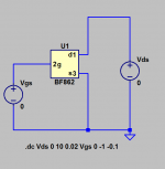
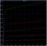
Change VTO in the NXP model from -0.57 to -0.7 and report back (that will get you in the ballpark.) The VI graph in the datasheet checks out well with my curve tracer.
Attachments
Last edited:
I tried again - still no joy I am afraid. If I comment out the subckt part it runs, but I don't trust the results. Any thoughts?
* BF862 SPICE MODEL MARCH 2007 NXP SEMICONDUCTORS
* ENVELOPE SOT23
* Adapted for generic spice programs 3-4-2014
.subckt BF862 1 2 3
Ld 1 4 1.1nH
Ls 3 6 1.25nH
Lg 2 5 0.78nH
Rg 5 7 0.535 Ohm
Cds 1 3 0.0001pF
Cgs 2 3 1.05pF
Cgd 1 2 0.201pF
Co 4 6 0.35092pF
J1 4 7 6 JBF862
*JBF862 model parameters:
.model JBF862 NJF(Beta=47.800E-3 Betatce=-.5 Rd=.8 Rs=7.5000 Lambda=37.300E-3
+ Vto=-.7
+ Vtotc=-2.0000E-3 Is=424.60E-12 Isr=2.995p N=1 Nr=2 Xti=3 Alpha=-1.0000E-3
+ Vk=59.97 Cgd=7.4002E-12 M=.6015 Pb=.5 Fc=.5 Cgs=8.2890E-12 Kf=87.5E-18
+ Af=1)
.ends
I put it together, ran it, and LTSPICE popped up a helpful error message telling me exactly what was wrong: the resistor "Rg" has an extra character string at the right end of the line. LTSPICE does not recognize this character string. When I deleted the string, I got the results shown below.
_
_
Attachments
I came across this project a little while ago, but have only gotten around to reading the whole thread this week. A huge thank you to Juma and everyone who has contributed  !
!
I'm going to start building this weekend. Should I go with the dual-rail version from way back, or the single-rail version as shown here ? Are there likely to be any differences in sound quality?
!I'm going to start building this weekend. Should I go with the dual-rail version from way back, or the single-rail version as shown here ? Are there likely to be any differences in sound quality?
AndrewT.
You don't stop to amaze me. You keep asking basic questions all the time and fail to understand simplest stuff but that doesn't stop you from "lecturing" scared newbies allthough you really know less than most of them, it's just your arrogant pose that makes them think that you actually know what are you talking about...
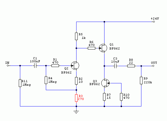
So not for you, but for those who will actually make something:
1. & 2. post #344, last sentence.
3. R2 is in the source circuit, so it does affect the gain.
4. R4 sets the gate reference for Vgs of the JFET. When R4 is connected that way, only R2 determines the Vgs of the Q2 but R3 still degenerates the Q2's source and affects the gain that way. That's why there is a positive voltage on the gate and we have to use the input cap. Of course, the source is more positive than the gate (Id x (R3 + R2) vs. Id x R3) so the JFET is correctly polarized this way.
Hehehe.
Nice preamp Juma
I put it together, ran it, and LTSPICE popped up a helpful error message telling me exactly what was wrong: the resistor "Rg" has an extra character string at the right end of the line. LTSPICE does not recognize this character string. When I deleted the string, I got the results shown below.
_
Thank you - I'll correct as proposed
I put it together, ran it, and LTSPICE popped up a helpful error message telling me exactly what was wrong: the resistor "Rg" has an extra character string at the right end of the line. LTSPICE does not recognize this character string. When I deleted the string, I got the results shown below.
_
Just ran the sim - it works correctly - thank you.
Guess I need to pay more attention to the error messages - lesson learnt!
there is an easier way to make this pre (see attached schematic).
Came to this thread looking for some gain before my (future) M2 and F5 build. The schematic quoted looks simple enough for me that I would want to try it.
My DAC turns out 4Vpp at -3dB, so to drive the M2 to max output, I am looking for a gain of 2-3. Inputs for both my F5 and M2 have 1kOhm resistors to the gates of the FETs and 100kOhm to ground.
I'd be grateful for some advice on the following questions:
1) Is it sufficient for this circuit to take the +24V from the power amps PSU (2x18V secondaries, 44mF-0.1Ohm-66mF per rail, ca 40mV ripple under load)?
2) If (1) is not advisable, would something shown to the right of R3 in this post work alright?
3) Given the high input impedance of the F5 and M2 front ends and the fact that this pre would sit in the same box, can I drop the buffer stage in the quoted schematic?
Thx!
1. I'm afraid not. PSRR of the circuit is not high enough for that....some advice on the following questions: ...
2. Yes. BC547c/BC550c based simple capacitance multiplier should deliver additional 40-50 dB of PSRR with only a volt or two of voltage drop. If that's not enough, an RC filter can be added into positive rail (10R in series + 1000uF to 10.0000uF cap to ground, before the cap. multiplier)
3. Sure. 1k Zout into 100k of Zin, within the same box, with short connecting cables, is more than good enough.

2. Yes. BC547c/BC550c based simple capacitance multiplier should deliver additional 40-50 dB of PSRR with only a volt or two of voltage drop. If that's not enough, an RC filter can be added into positive rail (10R in series + 1000uF to 10.0000uF cap to ground, before the cap. multiplier)
Whoa,
 thx Juma for the swift reply!
regarding (2), BC547c/BC550c means that I can use these instead of the BC548C stated in the original circuit, right? Or are you referring to a different schematic?
Is it critical to have +24V? B/c if I lose two more volts I will only have 20 or so Volts left.
Off to buy BF862...
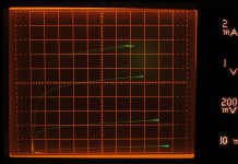
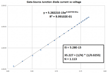
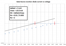
I just measured the forward bias characteristics of the Gate-to-Source junction diode of one single BF862 JFET. It may have been a weirdo freak device but ... this one's measured data is best-fit by the SPICE parameters
IS = 5.3E-15
N = 1.11
RS = 2.0
The NXP model displayed in Post #384 by member Bonsai, says
IS = 4.246E-10 (different by 5 orders of magnitude!!!)
N = 1.0
RS = 0.0
Let the buyer/designer beware
IS = 5.3E-15
N = 1.11
RS = 2.0
The NXP model displayed in Post #384 by member Bonsai, says
IS = 4.246E-10 (different by 5 orders of magnitude!!!)
N = 1.0
RS = 0.0
Let the buyer/designer beware
Attachments
I just measured the forward bias characteristics of the Gate-to-Source junction diode of one single BF862 JFET. It may have been a weirdo freak device but ... this one's measured data is best-fit by the SPICE parameters
IS = 5.3E-15
N = 1.11
RS = 2.0
The NXP model displayed in Post #384 by member Bonsai, says
IS = 4.246E-10 (different by 5 orders of magnitude!!!)
N = 1.0
RS = 0.0
Let the buyer/designer beware
a) isn't a lower gate-source current rather good news for the designer?
b) you got something wrong in the legend of the second graph
Thanks for the catch! Ohm's Law wanted me to calculate series resistance as R=V/I giving (1/2) ohm rather than 2 ohms. Kids let this be a lesson to you, don't perform datafitting in your bathing trunks, late on Sunday afternoon, in the pool cabana sipping a margarita.
It is indeed good news that the extrapolated zero-bias forward current is so low; lower even than the datasheet's specification VGSoff (1E-9 vs 5E-15), unless you're using the diode as a clamp and want accurate simulation of I vs V in forward bias. Maybe this guy, who's using three of them in series to prevent opamp saturation, might be one such person.
It is indeed good news that the extrapolated zero-bias forward current is so low; lower even than the datasheet's specification VGSoff (1E-9 vs 5E-15), unless you're using the diode as a clamp and want accurate simulation of I vs V in forward bias. Maybe this guy, who's using three of them in series to prevent opamp saturation, might be one such person.
Attachments

- Home
- Amplifiers
- Pass Labs
- BF862 Preamp