I'm interested. Let me know does it works.?Well, that's interesting. Hours after posting here the UPS man arrived with my left and right channel boards. EuroCircuits sent out 4 instead of 3. (Is it normal for them to send extras? This is only my second order from them, but the first one didn't have any extras.)
Anyway, assuming they check out this means I could have two sets available....
OK O K[emoji108]It'll probably take me a week or two to get things tested, but I'll let everyone know.
(If the boards have issues I'll be correcting them and ordering more, so folks can get in on that if they want. I'm also happy to share the Gerbers if anyone wants them.)
It'll probably take me a week or two to get things tested, but I'll let everyone know.
(If the boards have issues I'll be correcting them and ordering more, so folks can get in on that if they want. I'm also happy to share the Gerbers if anyone wants them.)

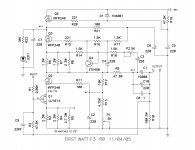
I'm trying to figure out if I got the orientation of P1 right.
P1 is used to set the output DC to the midpoint of the supply voltage. From a cursory examination of the schematic (attached), it looks like R6/R7/R8 + R12/R13/P1 act as a voltage divider, and that increasing P1 would therefore increase the output DC.
But the resistances of the R12/R13/P1 half of the voltage divider are way too high for that.
Looking at it some more, I think the "real" voltage divider is R12 + R13/P1, and that it's setting the gate voltage of Q2. In that case increasing P1 will increase the the gate voltage, opening the drain-source channel more and exposing the output DC more to R3/R4/R5, which will lower the output DC.
Or is there a third explanation that I'm still missing?
Thanks,
Jeff.
Attachments
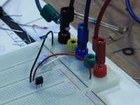
I measured my JFETs on a breadboard with 22awg hookup wire and got results somewhat higher than expected.
On a hunch I measured them again with mini-grabber test leads (18 or 20awg) and got numbers some 80mV lower (and in the expected range).
The 22awg wire wasn't heating up, and over a couple of inches it should be only a couple of miliohms. That doesn't seem like enough to slant things; are the breadboard connections a more likely culprit?
Yeah, I was forgetting that FETs have this middle "ohmic" mode where they respond to changes in Vds as well as Vgs. So the voltage passes through the cascode and changes the JFET's Vds.
They always respond to Vds, just less so in the "saturated" region.
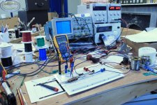
This first picture is just the overall setup so you can see the power supply and metering connections:

Here is the breadboard setup (heatsink removed for clarity):

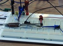
... and the mini-grabber setup (showing the heatsinking that was used in both):

The devices measure consistently in both setups; the numbers just don't agree between the two. If it were a dodgy connection, I wouldn't think it would show repeatable results?
Anyway, do the pictures give any clues?
Here is the breadboard setup (heatsink removed for clarity):
... and the mini-grabber setup (showing the heatsinking that was used in both):
The devices measure consistently in both setups; the numbers just don't agree between the two. If it were a dodgy connection, I wouldn't think it would show repeatable results?
Anyway, do the pictures give any clues?
Attachments
what's the fuss ?
either use proper pin clamping fixture , or solder wire to pins ..... everything else (just maybe) can be good .... or obviously not good , if showing any discrepancy
too much energy wasted in puzzling , instead of approaching things in proper engineering way
either use proper pin clamping fixture , or solder wire to pins ..... everything else (just maybe) can be good .... or obviously not good , if showing any discrepancy
too much energy wasted in puzzling , instead of approaching things in proper engineering way
google for pictures of breadboard underneath
then you'll see zillion of tiny wires , which resistance is good only for gate of LU
clamping fixture ..... sure that something as that exists")
transistor test socket - Google Search
then you'll see zillion of tiny wires , which resistance is good only for gate of LU
clamping fixture ..... sure that something as that exists
transistor test socket - Google Search
Oh cool; I like those 3M/Textool one-arm-bandit style ones.
http://ie.farnell.com/3m/216-3340-00-0602j/socket-ic-zif-16way/dp/9897330
http://ie.farnell.com/3m/216-3340-00-0602j/socket-ic-zif-16way/dp/9897330
I think (hope?) I'm getting near my final board layout.
I've changed the output caps since the big Panasonics are NLA: I'm using a pair of Wurth 8200uF electrolytics and a Mundorf 8.2uF polypropylene jelly roll.
I've also added a film cap (6.8uF polyester) to the Cmultiplier output.
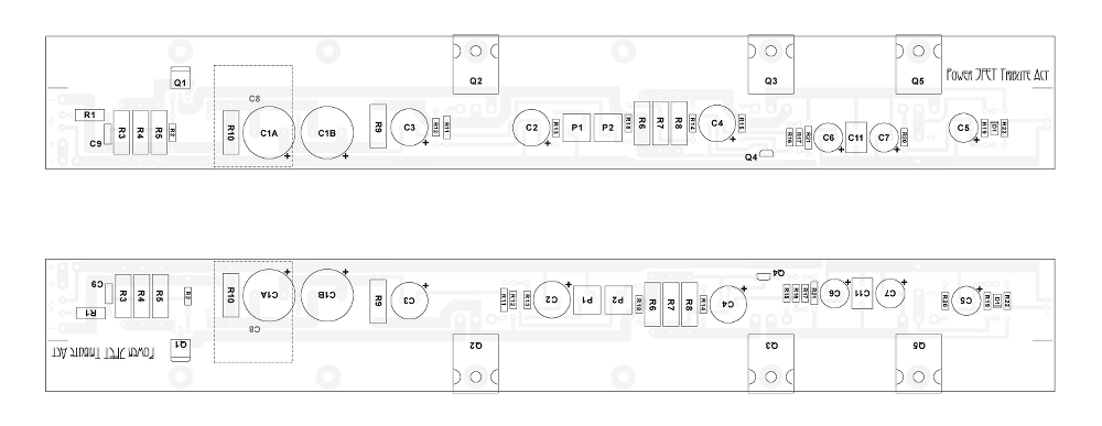
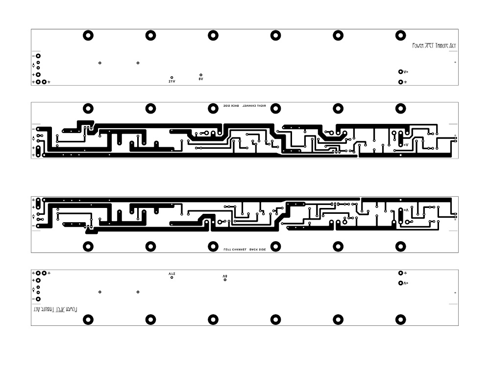
Nice artwork!
I'm busy designing the same kind of PCB's for different project in KiCad, and must also have a different left and right channel. Did you make the two channels from scratch and separate? Or is there something smart to do with flipping or mirroring and adjust the boards for pin-outs?
I have the right channel ready, but figuring out how to save work to make the left channel
Walter
Hi Walter,
I did my left and right channels from scratch (although using a single schematic file).
If you use a lot of zones you can make a copy of your right channel, Flip your zones to the opposite side of the board, and then do a Duplicate Zone onto Layer to get them back onto the correct side but mirrored. (You'll then need to delete the "extra" copy of the zone on the wrong layer.)
I suspect a block Mirror command wouldn't really help much as it would be harder to adjust for all the rotated footprints when all the tracks were there but in the wrong places.
I'll think about it some more, but even if I have an epiphany I won't be able to get it in soon as we're in feature-freeze for 5.0 right now.
Cheers,
Jeff.
- Home
- Amplifiers
- Pass Labs
- F3 Builders Thread