Did you add the 470 ohm source resistors?
Yes, I've tried that.Please see #3217
I just had a horrible thought.
Could the reason that the B1 sounds dull when compared to the faulty Pumpkins be due to the B&W DM683 tweeters being melted by 20MHz ?
A quick panic attack and a short test later - NO. The 683s are fine.
An amp capable of 20MHz full power bandwidth to pass it, is a very slim chance. How high was the oscillation peak to peak on the Pumpkin output anyway?
Drop the Alps in favor to a cheap DACT type switch pot. That will make it sharper subjectively.
Just to reiterate where we are.
Everything is still as per the schematic except:
R2 and R4 have been reduced to 2K7
There is a 2K7 between Q3(c) and Q4(c)
R5 and R6 are reduced to 27K
C1 and C2 are increased to 33pF
There are 2 x 33pF between Q1(g) and GND and Q2(g) and GND
There are two 4K7 load resistors between +OUT and GND and -OUT and GND.
IN+ IN- and SIG GND are shorted together.
JP1 is fitted shorting SIG GND to PWR GND.
I appreciate that C1, C2 and the two extras should be 15pF but I'm not spending any more money on this thing until I get somewhere.
R9 and R14 are now 470R.
It's still a wonderfully pure 9MHz oscillator.
An amp capable of 20MHz full power bandwidth to pass it, is a very slim chance. How high was the oscillation peak to peak on the Pumpkin output anyway?
Drop the Alps in favor to a cheap DACT type switch pot. That will make it sharper subjectively.
Yes, Thankfully the Aleph 4 saved the speakers.
Just a note, possibly slightly off topic.
I inadvertently shorted the ouput of the Aleph 4 - it was completely un-harmed.
I run this beast in a completely unprotected format relying upon the superior design to protect the peripherals. No relays, just pure HIGH CURRENT connections.
I inadvertently shorted the ouput of the Aleph 4 - it was completely un-harmed.
I run this beast in a completely unprotected format relying upon the superior design to protect the peripherals. No relays, just pure HIGH CURRENT connections.
Work finished early today 
Good, at least you now know the oscillation can be stopped.
Because the Pumpkin is balanced in and out, it therefor has two feedback paths, only one half needs to play up to cause problems on both sides.
What you need to do next is to turn it into an unbalanced pre - easily done.
With the inputs grounded and no links on R1 & R3, fit a shorting link across R7 (obviously with the power off) this will bias off Q7, the feedback will be via R5 only, power up and check J4, there should be no output unless there is something wrong with Q7, if there is - don't proceed with the next bit; check that Q2 gate is at 0V, if not - fit a link across R4; check for oscillation at J3.
Remove the links on R7 R4, repeat the above procedure with R8 R2 J4.
Don't feel too
You will get there in the end
2. Shorting R1 and R3 KILLS the oscillation . +IN and -IN are GROUNDED.
Good, at least you now know the oscillation can be stopped.
Because the Pumpkin is balanced in and out, it therefor has two feedback paths, only one half needs to play up to cause problems on both sides.
What you need to do next is to turn it into an unbalanced pre - easily done.
With the inputs grounded and no links on R1 & R3, fit a shorting link across R7 (obviously with the power off) this will bias off Q7, the feedback will be via R5 only, power up and check J4, there should be no output unless there is something wrong with Q7, if there is - don't proceed with the next bit; check that Q2 gate is at 0V, if not - fit a link across R4; check for oscillation at J3.
Remove the links on R7 R4, repeat the above procedure with R8 R2 J4.
Don't feel too
You will get there in the end
Last edited:
R1 and R3 are the input resistors. When you short these out, and then short the inputs, the amplifier is running at very high closed loop gain, so in effect the loop gain is very low. Under these conditions I would expect the oscillation to stop. This seems to suggest you have a loop stability problem.
at the moment Vbe from Q3 is 0,6V divided by R7 (0,47) equals 127mA for one side
you get 100mA by 0,6V divided by 100ma gives 0,6 Ohm......
you can read it in the chapter how shunty works......
http://dl.dropbox.com/u/20665608/The Pumpkin & Shunty.pdf
in much better English than mine.....
you get 100mA by 0,6V divided by 100ma gives 0,6 Ohm......
you can read it in the chapter how shunty works......
http://dl.dropbox.com/u/20665608/The Pumpkin & Shunty.pdf
in much better English than mine.....
Last edited:
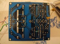
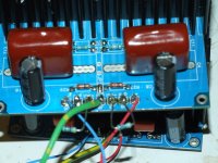
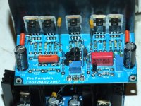
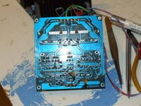
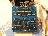
KatieandDad, can you post a high quality photo of your Pumpkin, top side and bottom side.
The components that are not hugging the boards are those that have been added during this conversation. I am trying very hard not to damage the delicate PCB.
Attachments
at the moment Vbe from Q3 is 0,6V divided by R7 equals 127mA for one side
0.6V divided by 127mA is....0.6 divided by 0.127, ...is 6 divided by 1.27,...is 4R7.
you get 100mA by 0,6V divided by 100ma gives..
0.6 divided by 0.1 is ... 6 divided by 1, is...?
(but then in much better English)
Last edited:
- Home
- Amplifiers
- Pass Labs
- Pumpkin preamp - ordered by Steen , official making thread