Whether you need matching or not depends on what you want to build.
If you want to build single ended, and use the Fairchild parts, then the N & P MOSFETS are NOT complementary (as I have posted years ago) and hence no matching is POSSIBLE. You can then enter into a philosophical debate as to whether you want transistors of the left channel and the right channel to be as identical as possible, or just rely on the circuit to compensate for the difference. I always match left and right channels for myself. But then I don't (have to) make these in production quantities.
If you build the balanced version, and use Toshiba MOSFETs (which are truely complementary, as I have also published here), and you want to cancel even order distortions as best as you can, then matched devices are a MUST. But of course you might not want to cancel ALL the even harmonics, but rather a mixture of 2nd, 3rd, 4th, ..... Then you should join the Swinger Club and swap until you get what you want, as Nelson suggested.
That's my opinion only.
And there are many other opinions, just as people would discuss endlessly how well you should match small signal JFETs for use in diff pairs.
Matched Quad N & P devices are not easy to obtain. You need a large pool to match from, or your "reject rate" is high.
I think the price asked for is not totally unfair, considering the effort.
I have just sold a set for less (curve tracer matched on heatsink), but that was my own stupidity.
Lucky guy, Dirk.")
Patrick
If you want to build single ended, and use the Fairchild parts, then the N & P MOSFETS are NOT complementary (as I have posted years ago) and hence no matching is POSSIBLE. You can then enter into a philosophical debate as to whether you want transistors of the left channel and the right channel to be as identical as possible, or just rely on the circuit to compensate for the difference. I always match left and right channels for myself. But then I don't (have to) make these in production quantities.
If you build the balanced version, and use Toshiba MOSFETs (which are truely complementary, as I have also published here), and you want to cancel even order distortions as best as you can, then matched devices are a MUST. But of course you might not want to cancel ALL the even harmonics, but rather a mixture of 2nd, 3rd, 4th, ..... Then you should join the Swinger Club and swap until you get what you want, as Nelson suggested.
That's my opinion only.
And there are many other opinions, just as people would discuss endlessly how well you should match small signal JFETs for use in diff pairs.
Matched Quad N & P devices are not easy to obtain. You need a large pool to match from, or your "reject rate" is high.
I think the price asked for is not totally unfair, considering the effort.
I have just sold a set for less (curve tracer matched on heatsink), but that was my own stupidity.
Lucky guy, Dirk.
Patrick
Last edited:
> but they did not have (allegedly) matching transfer curves as do the Tosh's...
What do you mean by allegedly ?
It was measured data published here openly for all to see.
http://www.diyaudio.com/forums/pass-labs/121228-f5-power-amplifier-17.html#post1507044
Patrick
What do you mean by allegedly ?
It was measured data published here openly for all to see.
http://www.diyaudio.com/forums/pass-labs/121228-f5-power-amplifier-17.html#post1507044
Patrick
Last edited:
But of course you might not want to cancel ALL the even harmonics, but rather a mixture of 2nd, 3rd, 4th, ..... Then you should join the Swinger Club and swap until you get what you want, as Nelson suggested.
Might be that its about distortion figures
But when Nelson mentioned J2 amp it was my immediate understanding that the "swapping" was about "matching" NPN to PNP
Those seems to me like the great unknowns
I can see the point with regards to balanced amps
But are they not mounted on each their own individual amp boards
Doesnt this again mean that lots of other factors influence the perfect balance
Looking at calculated probability with many unknown and uncontrolled factors its more likely that a mix of "lucky" imbalance will result in the perfect balance
That is to me what Nelson talks about
In which case only the matching of paralel devices seem to make any sense
...But when Nelson mentioned J2 amp it was my immediate understanding that the "swapping" was about "matching" NPN to PNP
Those seems to me like the great unknowns...
On the J2 that would only be P to P matching of the input differential jfets and then N to N at the output power jfets...
I believe J2 is with a single pair outputs, and why it was mentioned in relation to F5 not needing matched devices
Nelson suggested random "swapping" as being a good/only option, fore a single pair
Also that there seems to be no way to predict or calculate it, meaning completely random fore each amp/channel
At least thats how I understood it
If you match quads of 4 N and 4 P devices and split them in double pairs into left and right channel, and then claim that bias conditions will be the same fore each channel, that sounds like simple dreaming to me
But I admit to know way too little about these matters
Sure, I live in hoping too, and have bought devices matched with 3 digits numbers, to get the paralel devices right, within 0.001-0.003 tolerance fore each matched quad
Sure its fun to "believe" to have bought something very special
Tho, its a question if thats 100% reliable, or if it will change every time its measured
The stuff that dreams are made of
Patrick, whoa cowboy!
Yes, I see your curves - how were they generated?
How closely matched were the devices you tested, and how were they matched? (static bias, or dynamic curve tracer?)
I say allegedly because I only saw the Toshiba data sheets, had not seen your posted result. All the much better if they work like that!
Everyone else, this post by NP may shed some light on the matching/biasing/harmonics thing - from back in the thread a year or more:
NP on "the sweet spot"
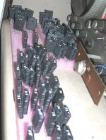
Btw, tinitus, here's the pix of the batch I had...
EDIT: what do you mean "within 0.001-0.003 tolerance "??
No matter what if one starts with closer tolerances it's more likely to get "textbook" or "simulation" like results than if things are all over the map. How that will sound is another matter entirely...
Yes, I see your curves - how were they generated?
How closely matched were the devices you tested, and how were they matched? (static bias, or dynamic curve tracer?)
I say allegedly because I only saw the Toshiba data sheets, had not seen your posted result. All the much better if they work like that!
Everyone else, this post by NP may shed some light on the matching/biasing/harmonics thing - from back in the thread a year or more:
NP on "the sweet spot"
Btw, tinitus, here's the pix of the batch I had...
EDIT: what do you mean "within 0.001-0.003 tolerance "??
No matter what if one starts with closer tolerances it's more likely to get "textbook" or "simulation" like results than if things are all over the map. How that will sound is another matter entirely...
Attachments
Last edited:
One of the advantages of DIY is that most of you have the
time and inclination to tweak the circuit that virtually no
manufacturer can devote. Yes, they often match devices for
one parameter such as Vgs, but that's it, and often this is
merely for current sharing or offset voltage.
There's more to device characteristics, and taking the time
to select devices for performance in the actual circuit is the
best way to get the most.
This does presume that you know what you want when you
see it. If a measured spec is the criterion, then your job is
easier than if you have to do extensive listening tests.
Hello everybody,
after reading all the thread, I started collecting parts to build a couple of F5 mono.
Last week I assembled the first (300VA 18-0-18, 27mFx3xrail, +24.1Vdc, -24.1Vdc, sk170BL, sj74BL, FQA12P20, FQA19N20C, mica and thermal paste, Peter Daniel board, no current and voltage limiter sections, resistor values as Pass scheme, alu hs 250x180x83mm).
First setup went smoothly, after a couple of hours, when bias was stabilized at 1.3A and offset at 0mV, I attached a speaker of no value and music flowed.
Another 2hrsx3 of testing and all was good, heatsink at 40°C behind the mosfets, mosfets case at 50°C. Then, when I turned it on the next day (from cold) I read immediately about 1500mV on both R11 and R12. I turned it off quickly, lowered pots to zero, did the setup again and I was able to get 600mV on R11-R12 stable with offset at 0mV.
Another couple of hours of continuing operation with no problems.
Next turning on from cold, today, same story. 1500mv on R11 and R12. I lowered again the pots, but now everytime voltage on R11 and R12 reach about 62mV, both increase abruptly to around 1500mV.
No parts burned, no smoke or something odd. I checked the passive parts, they are ok.
In the meantime I was testing the first mono, I assembled the other one (it's exactly the same). It works perfectly since the beginning, It's clear there's something in the first one that doesn't work properly, but I've no idea than rebuild the circuit with new active parts. I'd like to understand what happened. Have you any suggestion?
Last edited:
Btw, tinitus, here's the pix of the batch I had...
Well, mine are the less valued and cheaper Renesas
And from specs I thought they looked better fore multiple outputs
Unfortunately not knowing they were the wrong ones
Despite its not the right ones, its been confirmed they will work fine
2SK1058 / 2SJ162
It says Vgs(10V/100ma)
4x K1058 0.837 / 0.837 / 0.837 / 0.838
4x K1058 0.840 / 0.841 / 0.842 / 0.843
4x J162 0.500 / 0.501 / 0.504 / 0.505
4x J162 0.508 / 0.508 / 0.512 / 0.513
Not that I know exactly what it means
Oh, maybe that they are within 5ma, I dont know
But it was fun
I have changed my mind, and will either use the them as double pairs in F5, and have "safety" spares
Or use them all in BA-2
Not really decided
Thats how it is being a bit slow, things change before even started
And new things and ideas coming up
My suggestion would be to build F5 as standard with single pair Toshibas, or maybe two
And if you want more, look at BA-1 or BA-2
My decision was based on too little knowledge, and excitement
Lack of common sense might not be the best conditons
But its ok, I dont regret it, its been a learning process, small but still something
M.M
I have seen this happen to my F5 with circuit protection inserted, although not as high a voltage spike. If the voltage settles then there is no issue.
Notice that if you blow cold air over the circuit, the voltage reading raises and lowers.
.62v from .59v is not that much of a change to be worried about. Also, you will have to reset the pots after some break in time.
Maybe someone else with more experience can verify this.
Hi Tinitus,
have you seen this thread?
May be the best way to use your renesas.
http://www.diyaudio.com/forums/pass-labs/162042-f5-meets-buzquito.html
have you seen this thread?
May be the best way to use your renesas.
http://www.diyaudio.com/forums/pass-labs/162042-f5-meets-buzquito.html
Thanks bobo, thats great
I did miss that one, inspiration from france, it seems
Need to study it carefully
Not sure, but could BA-2 actually also be the one, with different bias design
A power buffer with high gain preamp, maybe
Being symmetric in both channels might tell something, just not to me, sorry
Well, its just to keep the focus on your problem
I did miss that one, inspiration from france, it seems
Need to study it carefully
Not sure, but could BA-2 actually also be the one, with different bias design
A power buffer with high gain preamp, maybe
Then, when I turned it on the next day (from cold) I read immediately about 1500mV on both R11 and R12.
Being symmetric in both channels might tell something, just not to me, sorry
Well, its just to keep the focus on your problem
Being symmetric in both channels might tell something, just not to me, sorry
not exactly symmetric, negative rail more than positive, an offset of about -200mV was generated.
ThanksWell, its just to keep the focus on your problem
perfect opportunity to replace crystal ball with little mosfet testing setup

I found this cute little test. Only uses a DMM
This testing procedure is for use with a digital multimeter in the diode test-range with a minimum of 3.3 volt over d.u.t. (diode-under-test)
Connect the 'Source' of the MosFet to the meter's negative (-) lead.
1) Hold the MosFet by the case or the tab but don't touch the metal parts of the test probes with any of the other MosFet's terminals until needed.
2) First, touch the meter positive lead onto the MosFet's 'Gate'.
3) Now move the positive probe to the 'Drain'. You should get a 'low' reading. The MosFet's internal capacitance on the gate has now been charged up by the meter and the device is 'turned-on'.
4) With the meter positive still connected to the drain, touch a finger between source and gate (and drain if you like, it does not matter at this stage). The gate will be discharged through your finger and the meter reading should go high, indicating a non-conductive device.
Such a simple test is not 100% -- but is useful and usually adequate.
> How closely matched were the devices you tested, and how were they matched? (static bias, or dynamic curve tracer?)
I took two random sample out of my measurements, and the Vgs values were stated in that post. They were measured dynamically using a functions generator to drive Vgs with 100Hz triangular wave (with variable DC offset) and Vds supplied by a lab supply, on heat sink, after 10 minutes steady state, i.e. exactly working conditions in the real circuit. 1000 measurement points per device.
I take my matching seriously.
Patrick
Last edited:
Hello everybody,
after reading all the thread, I started collecting parts to build a couple of F5 mono.
Last week I assembled the first (300VA 18-0-18, 27mFx3xrail, +24.1Vdc, -24.1Vdc, sk170BL, sj74BL, FQA12P20, FQA19N20C, mica and thermal paste, Peter Daniel board, no current and voltage limiter sections, resistor values as Pass scheme, alu hs 250x180x83mm).
First setup went smoothly, after a couple of hours, when bias was stabilized at 1.3A and offset at 0mV, I attached a speaker of no value and music flowed.
Another 2hrsx3 of testing and all was good, heatsink at 40°C behind the mosfets, mosfets case at 50°C. Then, when I turned it on the next day (from cold) I read immediately about 1500mV on both R11 and R12. I turned it off quickly, lowered pots to zero, did the setup again and I was able to get 600mV on R11-R12 stable with offset at 0mV.
Another couple of hours of continuing operation with no problems.
Next turning on from cold, today, same story. 1500mv on R11 and R12. I lowered again the pots, but now everytime voltage on R11 and R12 reach about 62mV, both increase abruptly to around 1500mV.
No parts burned, no smoke or something odd. I checked the passive parts, they are ok.
In the meantime I was testing the first mono, I assembled the other one (it's exactly the same). It works perfectly since the beginning, It's clear there's something in the first one that doesn't work properly, but I've no idea than rebuild the circuit with new active parts. I'd like to understand what happened. Have you any suggestion?
I do not know, but I can guess... but let me ask first, does this happen on two channels the same way and amount?
But I think you said it was the first... what may be happening is that the two Mosfets you chose to use are on "opposite" ends of the usual Vgs spread. No matter if that is a cause or not, they seem to drift different amounts from cold. Since you bias them when hot, they are fine - but then when they are cold they move "back" a different amount, thus the large offset.
IF this is what is going on you've got two main choices:
- make a simple test jig to determine the Vgs of the devices you have and try to put the ones that are closest to each other on the same board (or get some more devices and test and pick a better set of pairs). Actually the amp itself is sort of a test jig... you can set up a meter on the gate drive line and measure the voltage that way. (also you can test now what the Vgs is cold for 0 offset vs hot and see what the difference in absolute range is between P & Nch)
- or use the circuit suggested earlier or one like it to servo control the DC offset. In that case the static values would be chosen so that the cold bias setting causes the amp to have limited offset.
This is assuming that something else isn't a wrong value or miswired or otherwise malfunctioning...
_-_-bear
> How closely matched were the devices you tested, and how were they matched? (static bias, or dynamic curve tracer?)
I took two random sample out of my measurements, and the Vgs values were stated in that post. They were measured dynamically using a functions generator to drive Vgs with 100Hz triangular wave (with variable DC offset) and Vds supplied by a lab supply, on heat sink, after 10 minutes steady state, i.e. exactly working conditions in the real circuit. 1000 measurement points per device.
I take my matching seriously.
Patrick
Ya.
Ok, so then how did you record the graph?
_-_-bear
2 channel, 16-bit Digital oscilloscope.
You can of course also use a 24-bit sound card if you can take care of the intrinsic AC-coupling problem.
We also have a curve tracer from Locky_z which we are modifying with improvements for long-term stability.
But that will take a bit longer with too many projects running in parallel.
P.
You can of course also use a 24-bit sound card if you can take care of the intrinsic AC-coupling problem.
We also have a curve tracer from Locky_z which we are modifying with improvements for long-term stability.
But that will take a bit longer with too many projects running in parallel.
P.
Don't forget that the JFETs have their own set of thermal issues. I don't know how they are oriented on Peter's boards...I've gotten the amplifier to work within spec with GR and BL devices, but I am pretty relaxed on the layout of my boards, preferring not to crowd devices together. In fact, for all of my F5's I have Caddock's mounted to the heat sinks! You may also have the 0.47R source resistor or 2x100R feedback resistors cooking the JFETs.
As has been mentioned before, the Fairchild MOSFETs are NOT complementary devices. I use them in my F5's with the protection circuitry and have not had problems with offset (but patience is its own virtuous reward in setting up the bias and offset.)
With regard to matching devices -- I found out early on and it's probably on the F4 thread -- devices with matched Vgs from the same lot often exhibit the same or very close transconductance.
- Home
- Amplifiers
- Pass Labs
- F5 power amplifier