Nelson pcb,
And when are these little Nelson Pass pcb's going to be available? I would like about 4 of them.
On another note. What is the preferred method of utilizing jfets in the input section when the voltage available is beyond the fjets range. Many members have their own ideas on this ie, resistor, cascode, series with mosfet etc. Which works best? Thanks. Tad
h_a said:not a Toshiba part
Same Toshiba part, but a special edition with goldplated leads.
The A-types were for sale briefly, but at 10 times the cost of the regular version.
And when are these little Nelson Pass pcb's going to be available?
Master says soon. So somewhere this year?
What is the preferred method of utilizing jfets in the input section when the voltage available is beyond the fjets range
You can just cascode it - with whatever you want (bjt, mosfet, jfet). The resistor you mention is the load and will not ensure that the jfet sees sufficiently low voltage.
Have fun, Hannes
> I'm waiting for Nelson's pcbs. Sure I could do my own, but having at least a single Nelson Pass piece is a bit special
This place is called DIY Audio ??
> I'm still thinking of the Toshibas, it's just that I have more than enough Fairchilds already at hand...
Why not just build the Fairchild first ?
Then you can always decide to swap the Toshibas in later on.
Patrick
This place is called DIY Audio ??
> I'm still thinking of the Toshibas, it's just that I have more than enough Fairchilds already at hand...
Why not just build the Fairchild first ?
Then you can always decide to swap the Toshibas in later on.
Patrick
EUVL said:> I'm waiting for Nelson's pcbs. Sure I could do my own, but having at least a single Nelson Pass piece is a bit special
This place is called DIY Audio ??
.......
Patrick
you forgot smiley there .
maybe someone wants 4 Papa's pcbs to hang them on wall , as pride and joy ?
EUVL said:[BIn any case, don't do armchair DIY...
Patrick [/B]
For that I have a powerhouse of researchers, experimenters and developers that include you, NP, JC, BC, etc...throw in JaccoV when you're going through your parts list and you want a good laugh...then I start building
")
Thank you.
This place is called DIY Audio ??
Ja!!
C'mon! One fetish piece of his Passness is a must!
The other zillions of pcbs I've still to do myself.
Have fun, Hannes
By the way: maybe somebody wants to work out a nice jfet only JLH with LU1014 in the output? I have such a feeling that mine will never be finished....
By the way, could somebody tell me what the limiting factor for the F5's power into 2R is?
Fig. 10 in the article shows clipping at 50W into 2R - at this power the F5 already left ClassA (5 A output current), but didn't not yet approach the rail (10 V output voltage).
What's happenin here?
Have fun, Hannes
Fig. 10 in the article shows clipping at 50W into 2R - at this power the F5 already left ClassA (5 A output current), but didn't not yet approach the rail (10 V output voltage).
What's happenin here?
Have fun, Hannes
Safe Operating Area limits of the MOSFETs. At least that's what I take it Papa means when writing: "The amplifier with 24 supply rails should be good for a 50 watt peak into 8 ohms, or about 2.5 amps. For a 4 ohm load we would want 5 amps, and for a 2 ohm load, we want 10 amps. Since we only have two output devices, we probably are best off stopping there."
jacco vermeulen said:Actually, i was thinking of using the F5 boards as body jewelry at the nudy beach.
Single Ended, of course.
Hardly expeditious......all that wasted space!

Has anyone come up with replacements for te 2sk170 and 2sj108... and the one alternative given for each by Nelson?
My boards are 55mm x 130mm, virtualy fully semetrical, with the outputs about 100mm appart.
The 2sj108 and its alternative specificaly seem to be hard to find...
My boards are 55mm x 130mm, virtualy fully semetrical, with the outputs about 100mm appart.
The 2sj108 and its alternative specificaly seem to be hard to find...
Attachments
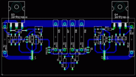
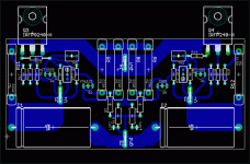
I would perhaps move the power supply connections to the bottom left and right corners to aviod any voltage difference between the common nodes of the MOSFET source resistor and the JFET drain resistors. Also makes it easy to double up to a balanced on one PCB. And for that matter perhaps use a soldered jumper to connect the 10R (for which I use 3x 33R 0.25W in parallel) JFET source resistors to Gnd, which allows you to convert to an X-Balanced later. All options then open.
Otherwise quite well done, I thought.
Patrick
Otherwise quite well done, I thought.
Patrick
Hi thanks for the reply...
I thought about cornering the two power points, but decided to stick with the stared layout giving all components accesing those nodes, connection at a single (reference) point, in the same way you might be used to seeing ground stars. It has the benefit of not makeing high and low current paths shareing the same tracks... (Quieter operation)
I do not see myself going balanced soon, but I will try to find the balanced schematic in this long thread, to get a grasp of what you intended wit the 10R's.
Also, I still need to sim the boards to check dissipation etc, so it will likely still change a little...
- Home
- Amplifiers
- Pass Labs
- F5 power amplifier