I'm going to go out on a limb and predict that you have a measurement error
as usual....
as near as I can figure, that particular mosfet was heated up a little when I re-soldered the wires to the terminal block I was using as a test jig. The mosfet was dumping heat to the heatsink it was pressed against faster than it was heating up. Hence, Vgs went up as I watched.
for anyone who didn't notice and who has a pile of IRF240's laying around (and I can't imaginine why any Passaficianos would have those......
 ) -- Mouser has the SFH9240's in stock, and they are inexpensive.
JJ
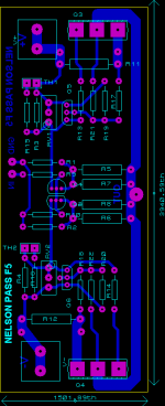
Very nice layout Juma!
Very nice layout Goffe!


I have etched my boards and started populating them, but a funny thing happened to me on the way to mounting the output devices and drilling the heatsinks ... I got this crazy idea and I blame it all those crazy fools in the full-range forum ... I put everything on hold for now to build a CNC router table
I'll be back one day to complete my F5, hopefully before summer's out

Very nice layout Goffe!
I have etched my boards and started populating them, but a funny thing happened to me on the way to mounting the output devices and drilling the heatsinks ... I got this crazy idea and I blame it all those crazy fools in the full-range forum ... I put everything on hold for now to build a CNC router table
I'll be back one day to complete my F5, hopefully before summer's out
Re: JUMA PCB
It's Sprint-Layout 5.0 (http://www.abacom-online.de/uk/html/sprint-layout.html) - 40 EUR only
mithomas said:JUMA,
What software did you work with?
It's Sprint-Layout 5.0 (http://www.abacom-online.de/uk/html/sprint-layout.html) - 40 EUR only
twitchie said:Very nice layout Juma!
Very nice layout Goffe!
I have etched my boards and started populating them, but a funny thing happened to me on the way to mounting the output devices and drilling the heatsinks ... I got this crazy idea and I blame it all those crazy fools in the full-range forum ... I put everything on hold for now to build a CNC router table
I'll be back one day to complete my F5, hopefully before summer's out
It took me a weekend to build one: The Elektor Conlinbus Profiler.
Should let you get back to the real interesting F building activities real quickly.
Re: JUMA PCB
Mike, you don't need t no itching kit read this:
http://www.diyaudio.com/forums/showthread.php?postid=1073081#post1073081
mithomas said:
Anybody got any recommendations on an Etching kit in the states?;otherwise, I will wire this Point to point.
Mike
Mike, you don't need t no itching kit
read this:http://www.diyaudio.com/forums/showthread.php?postid=1073081#post1073081
Re: Re: JUMA PCB
Read the thread which Juma cites -- you can get 2% H2O2 as an antiseptic in the drug store, and muriatic acid (for cleaning brick at the hardware store).
The F5 design is so spare in the number of parts there's no reason it couldn't be put together on RS proto-typing boards.
juma said:
Mike, you don't need t no itching kit
http://www.diyaudio.com/forums/showthread.php?postid=1073081#post1073081
Read the thread which Juma cites -- you can get 2% H2O2 as an antiseptic in the drug store, and muriatic acid (for cleaning brick at the hardware store).
The F5 design is so spare in the number of parts there's no reason it couldn't be put together on RS proto-typing boards.
JUMA post
Juma, thanks,
Okay,
So I will try to spell it out for myself..
so your method is to tape on printout for drilling holes (got to find real tiny bits, hmmm)
Then I suppose take this printout off and then handraw the circuit with a marker of the copper PCB sheet. What type of water proof marker should I use, not a Shapie permanent marker I suppose? More like a crayon?
Add into Hydrogen peroxide and Muratic acid solution.
Then add flux, and then solder the traces on I would assume with some real wide Solder with a wide tip iron. Sounds like cooking...
It will then look like my old Hafler DH-200 boards.
Did I misunderstand something?
Mike:
THis questions has been askd a couple of times...I searched the thead, but do not really understand the correct answer, so please be patient with me:
As the bridged version of the F4 sounded so much better on my speaker:
Can I simply use two F5 as a bridged amp without any changes (like in the F4) ?
If not: What needs to be changed ?
THX a lot
As the bridged version of the F4 sounded so much better on my speaker:
Can I simply use two F5 as a bridged amp without any changes (like in the F4) ?
If not: What needs to be changed ?
THX a lot
What type of water proof marker should I use, not a Shapie permanent marker I suppose?
I believe that a Sharpie type marker is exactly what they use..
After, you scrub it off using I dunno - laquer thinnner?
Variac said:
I believe that a Sharpie type marker is exactly what they use..
After, you scrub it off using I dunno - laquer thinnner?
Sharpie works fine. Clean the board with a brillo pad and then use a degreaser . Draw your pattern with the sharpie and etch with 2 parts peroxide and 1 part muriatic. Be careful with the mixture ..I do the etching outdoors. When etch is complete wash board well and drill holes. Then I coat the traces with flux from flux pen from mouser and let flux dry. Then I flow solder on the traces.
I have also drilled holes first but that requires laying traces out twice.
The reason for flux solder treatment is to cover pinholes after etch. The sharpie is not the greatest mask. You might do better with Babo's oil paint .I imagine a tube of artist's oil would do the job.
sandstorm33 said:I imagine a tube of artist's oil would do the job.
"We take our obsolete technologies and turn them into art"
- Marshall McLuhan
Home-made PCBs
Guys, this is how I do it:
- You print on paper the published picture (it's a bottom view of the PCB - take care with dimensions)
- Scotch tape the piece of paper over the cleaned copper surface
- Drill the holes
- Clean it again (acetone, nail polish remover...)
- Use the water-resistant permanent marker (Staedtler, Faber-Castel...), with a, preferably, hard tip sized 1 mm or smaller to draw the traces exactly like they are on the paper you used for drilling
- Now you etch it like described ( H2O2 + HCl )
- Clean the marker traces with acetone
- Cover the copper traces with non-acid soldering grease (that's the name used here - I don't know the name of US equivalent - it's a greasy substance that makes soldering easier and quicker)
- Use a small quantity of soldering tin to cover the traces
- Clean the grease (alcohol, acetone, dish-washing detergent...)
Your PCB is ready. The success mainly depends on how clean the copper is before the drawing - don't touch it with your fingers.
One more thing: No brillo-pads or similar stuff - no abrasive materials - we don't want to mechanically hurt the copper traces. Acetone on cotton-ball and detergent on soft sponge will do the cleaning perfectly.
Nelson Pass said:You can do that, no changes. Just drive each input with the
opposite polarity of the same signal.
Thanks, Nelson, I will start the work immediately, last question: is the heat dissipation similar to the F4 or much lower or much more ?
So, could I get two F5 (so four channels) into a case which would require normally one F4 (two channels)...?
- Home
- Amplifiers
- Pass Labs
- F5 power amplifier