current feedback or not?
Now, having read the article, I' like to get back to one of Papa's statements: "The feedback mechanism for this amplifier is R3 through R6, a dual pair of low impedance voltage dividers which feed the output to the Source pins of Q1 and Q2. Low impedance feedback has been (incorrectly) referred to as 'current feedback'"
Is this to be understood as a general critique on the term (which actually is a misnomer of sorts), or does it refer to that specific amp, meaning that this amp doesn't fall into that category, regardless of semantics?
My take would be the former, as I still tend to see the amp as a cleverly simplified and specialized current feedback operational amplifier.
Any comments?
- Klaus
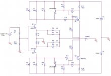
Sorry guys i am trying to simulate the circuit with PSpice but probing the current on the input jfets it says 10mA are flowing instead of the supposed 6mA.
Here is the schematic i am using (i also tried to use the 2sj74 and 2sk170 but i get the same results)
Do you see any mistake?
Could it be some error on the models? (in case may somebody post the spice model for the parts used?)
thanks a lot.
Here is the schematic i am using (i also tried to use the 2sj74 and 2sk170 but i get the same results)
Do you see any mistake?
Could it be some error on the models? (in case may somebody post the spice model for the parts used?)
thanks a lot.
Attachments
Stefanoo said:Sorry guys i am trying to simulate the circuit with PSpice but probing the current on the input jfets it says 10mA are flowing instead of the supposed 6mA.
Here is the schematic i am using (i also tried to use the 2sj74 and 2sk170 but i get the same results)
Do you see any mistake?
Could it be some error on the models? (in case may somebody post the spice model for the parts used?)
thanks a lot.
I think your assumed values for P1, P2 , R15,R16 are in error. All four are variable in an effort to maintain the 4+ volts across the 2.2k R3/R4.
Maybe I misunderstand here, but from what I understand from the article, you don't adjust P1=P2, but rather you adjust them independently to get minimal dc offset as well as maintaining 0.59 volts across R11 and R12
Quote from the article:
For each channel you will be adjusting P1 and P2 alternately in order to achieve 0 volts DC at the output and .59 volts across R11 and R12. Each time you adjust P1 you will probably have to go back and adjust P2 again, and so I recommend adjusting the pots in half-measures, alternately setting the pots half-way to their voltage goals and measuring the DC values.
Unless there is something very wrong, when the output is at 0 V DC, the values across R11 and R12 will be equal.
Stefanoo said:10mA current flowing on the jfets, is this a correct?
Question : what good would a Spice model for a JFET be if it could only be used at a fixed Idss value ?
Stefanoo said:i guess not too much.
But, what has to do with the simulation? what do you mean?
Do you have any suggestion?
that means that simulation is here to help you to understand how thing works , and then you must learn from books, schematics , ppl , and real work ;
sims can't make you Papa .
yes, you are right.
That is why i am re-reading all my scrap books of Electronics from the University.
I guess i need to refresh many things as i have abandoned them in these years (not completely....but i am no longer able to do the things i used to do in such a simple manner).
Few days and my recap will be done....yuuupppieee!!
Obviously....even though a simple circuit can be figured out by a couple of calculations...i still think simulations are useful.
An example?
As i was building the output attenuator for the Aleph P, I had at that time the model simulated on my computer.
As i had to decide the value of the resistors for the 24 stepped attenuator i based the calculations on the simplest logarithmic law feeling sure since everybody did that using that excel table.
When i wired up the attenuator and plugged it in i realized that output voltage wasn't what i expected to be.
Why?
Because i didn't take in consideration that since low feedback value of the network is used, output impedance of th circuit isn't constant with the load and this messed up ALL the calculation...and thus the output volume control was a disaster from my view point.
So, i simulated the 24 steps trying the different values available till finding the right values that gave me what i needed.
This time i wired up the attenuator again with the new values ....plugged it in the circuit..and..no surprise on the test bench.
Result? the output volume control is now perfect.
No audible gab when switching position but only a linear audible variation.
Conclusion: if i would have simulated this last part from the beginning i would have saved lots of time and few money since i had to re-buy the resistors.
So never think to be too good for the simulator.
this is my personal thought.
Not even if you are a master degreed engineer who got the highest score...as i think many of you guys are...
i think....unless you have a big practice to be able to see things from far away....i think you might need a neutral confirmation that your ideas are correct....unless you are Nelson Pass...of courseeee....
so after this blameless post....is there anybody that might kindly help me to figure out why is my simulation going wrong?
Stefanoo said:.........
so after this blameless post....is there anybody that might kindly help me to figure out why is my simulation going wrong?
I'm not talking/writing anything against sims ;
answer is simple - if you put correct parts values in proofed schematic , then model of active device isn't good enough .
period
that is what i think as well.
I have posted the schematic i am using in case you guys would see some mistake.
If no mistake on the actual draw then it must be something wrong on the models..i guess.
So, may anybody post here the spice model for the jfet and irf parts?
thanks.
I have posted the schematic i am using in case you guys would see some mistake.
If no mistake on the actual draw then it must be something wrong on the models..i guess.
So, may anybody post here the spice model for the jfet and irf parts?
thanks.
Stefanoo said:what do you mean?
Your JFETs have an apparent resistance, if you put a source resistor behind it you can vary the current flowing into the drain.
But the actual current is determined by the Idss value of the device at hand.
Whether you play The-Sims or Curl-Ball with real devices, Idss is your input, different input is different output.
(NP suggested 8mA-Idss parts several pages back, which leaves over 6mA with the source resistor value in the schematic.)
sorry jacco i don't get your suggestion.
i should add a resistor at the source of each the jfet where there is the two 10ohm resistors that regulated the gain of the second stage?
i am very ignorant as you can see if you could kindly explain me a bit more what you are trying to say i will appreciate it..
more if you or anybody else have a good spice model to share ...is obviously welcome.
i should add a resistor at the source of each the jfet where there is the two 10ohm resistors that regulated the gain of the second stage?
i am very ignorant as you can see
if you could kindly explain me a bit more what you are trying to say i will appreciate it..more if you or anybody else have a good spice model to share ...is obviously welcome.
Regulated power supply
Hi,
I am thinking of regulated PSU for F5. Regulated ZenV5 PSU is one way to go, but I want simpler. What about LT1083? It has 7.5A cont. current rating and within Vin-Vout <= 5V, it has cca 10A peak. I guess this would do...
... and I do not plan to put much capacitance after regulator, only one 4.7uF (polyester/polypropene).
What do you think? It's simple and should be good.
Matej
Stefanoo said:trying to say :
Your JFET models are set up for 12mA Idss, Spice models have NIENTE parameter spread.
Re: Regulated power supply
I planned to just use two Plitron 300va 2x18vac transformers (per amp) that I used in F4 with full wave bridges and CRC each for plus and minus rails. With the F4 load it yields a little more than +/-24vdc and seems pretty stiff, so I was hoping this would be adequate for F5 (6a continuous, 10a peak per channel) and keep the operating point where it is supposed to be for lowest distortion. Seems like a pretty simple solution unless noise sensitivity is just really high. I will probably do as the natives do and "just try it" except I really hate to take apart my F4 to find out.
Tom
In the article, Nelson said unregulated supplies work just fine though you could choose to use Z3 or Z5 as examples of regulated ones. The Z5 itself is apparently very sensitive to supply line noise, but I'm not sure whether the F5 is quite as sensitive (requiring regulation).matejS said:Hi,
I am thinking of regulated PSU for F5. Regulated ZenV5 PSU is one way to go, but I want simpler. What about LT1083? It has 7.5A cont. current rating and within Vin-Vout <= 5V, it has cca 10A peak. I guess this would do...
... and I do not plan to put much capacitance after regulator, only one 4.7uF (polyester/polypropene).
What do you think? It's simple and should be good.
Matej
I planned to just use two Plitron 300va 2x18vac transformers (per amp) that I used in F4 with full wave bridges and CRC each for plus and minus rails. With the F4 load it yields a little more than +/-24vdc and seems pretty stiff, so I was hoping this would be adequate for F5 (6a continuous, 10a peak per channel) and keep the operating point where it is supposed to be for lowest distortion. Seems like a pretty simple solution unless noise sensitivity is just really high. I will probably do as the natives do and "just try it" except I really hate to take apart my F4 to find out.
Tom
- Home
- Amplifiers
- Pass Labs
- F5 power amplifier