I don't know how you did your Idss measurements but they are wrong,
if you have genuine LSK170a and LSJ74a parts.
Your R2/R3 measurements, however, show about ~2.4mA and are consistent with
low Idss a-grade parts (Idss range 2.6mA to 6.5mA)
The F5 really should be built with higher Idss parts (B for Linear/BL for Toshiba).
If you don't want to get new parts, then you can consider parallel parts with
the other LSK/LSJ you have.
But I would properly measure their Idss first before doing this.
These are clear fakes, toshiba never make any 2SK170 with Idss > 20mA. Probably J112 or J113.2SK170 -N-FET - 24-28mA --on the JFets ---2SK170_BL-2I
This you need to verify Vp < 0.22V. If Vp > 0.8V it could be 2SJ103GR.2SJ74 -P-FET - 2,78-3,02mA --on the JFets ---2SJ74_GR-4K
Your data is confusing you have grade A fets with grade F printing, something is obviously wrong, not sure what happened.LSK170A -N-FET - 11,7mA --on the JFets ---LSK170_F-1529C
LSJ74A -P-FET - 38,4mA --on the JFets ---LSJ74_F_1412C
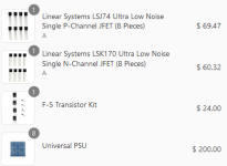
From Linear Systems Matched JFETs – diyAudio Store :
From LIS datasheet:JFET SPECIFICATIONS
Product data: LSK170 LSJ74
Grades
A (equivalent of Toshiba Gr), Idss ranging from 2.6-6.5
B (equivalent of Toshiba Bl), Idss ranging from 6.0-12.0
C (equivalent of Toshiba V), Idss ranging from 10-20
D (no Toshiba equivalent), Idss ranging from 18.0-30.0
I don't have any data on grade F.
Are you sure you made Idss measurement correctly?
Last edited:
hello dear community,
I have a F5 since 2018 and I´m happy-- standard JFET and 2SK1058/2SJ162
The Idss range of the JFETs (A) you selected are correct for lateral MOSFETs, almost perfect actually. A is not an indicator of quality, it indicates the Idss range, A being the lowest. I'm sorry if you already knew that. However your reading of dozens of mA on some parts is plain wrong. There's no way you can get that much current through these devices, unless there's a damaged device.
They are also absolutely not appropriate for Vertical MOSFETs. Your Idss readings are also not consistent with the JFET source resistor readings. We can estimate the JFETs running about 2.4mA, which would be about a third of the target Idss for the schematic, but otherwise spot on for the A graded devices.
If you are loath to make any major changes, you can simply increase the drain resistance by using a larger trimmer and/or omitting the parallel resistor completely. A 4k7 drain resistance with 2.4mA will result in a bias of 11V, which is a lot more than what you need. OTOH your 4.2V reading of Vgs point to a combined drain resistance of 1.75k. There's a few contradictions in the numbers you're posting, so taking a step back will allow more focused help.
May I suggest you post a schematic here and put down your part values and voltage readings? The 320mV you quote points to you already hitting half the target bias (and it goes up quickly from there) with a quarter of the JFET current so you're looking good overall.
Hello again,
my journey throu this all:
1) order JFet B-grade an but it in with all corrected restistors according to original schematic.
2) put in operation and on my left channel (goal for R7/R8 was 0,7V or max 0,8V) i turn too fast my poti and about 1,2V they run away I´m a idiot)
3) order set of MOSFET waiting...
4) put in operation, and set both channels to 0,7 volts
first run to set dc offset --3 hours shut down
2nd run 5 hours and my DC offset about -1,6mV to +1,8mV
I ran about 5 long test in 3 days to optimice my dc offset and finally a dc offset about -0,9mV to +1mV was very OK for me.
5) shorten all cables and connections carfully
6) put in operation --- after 8 seconds R13 gate resistor of Q3 was sending a light!! damage of all 2 Mosfets
I´m a electronic engineer but this is to much for me, cause i checked all several times at it was running 3 days and now this again??
I recognize also, that if I switch on the F5 the R7/R8 voltages always runs up to about a max. of 0,9V and go down to within 20 seconds to 0,66V and after heating up the stabilize to 0,702V or so......
is the bias to high for this vertival MOSFets???
thanks in advance for your comments and suggestions
regards Harry
my journey throu this all:
1) order JFet B-grade an but it in with all corrected restistors according to original schematic.
2) put in operation and on my left channel (goal for R7/R8 was 0,7V or max 0,8V) i turn too fast my poti and about 1,2V they run away
I´m a idiot)3) order set of MOSFET waiting...
4) put in operation, and set both channels to 0,7 volts
first run to set dc offset --3 hours shut down
2nd run 5 hours and my DC offset about -1,6mV to +1,8mV
I ran about 5 long test in 3 days to optimice my dc offset and finally a dc offset about -0,9mV to +1mV was very OK for me.
5) shorten all cables and connections carfully
6) put in operation --- after 8 seconds R13 gate resistor of Q3 was sending a light!! damage of all 2 Mosfets
I´m a electronic engineer but this is to much for me, cause i checked all several times at it was running 3 days and now this again??
I recognize also, that if I switch on the F5 the R7/R8 voltages always runs up to about a max. of 0,9V and go down to within 20 seconds to 0,66V and after heating up the stabilize to 0,702V or so......
is the bias to high for this vertival MOSFets???
thanks in advance for your comments and suggestions
regards Harry
Burning of gate resistor indicates parasitic oscillation, and usually needs small capacitors across the feedback resistors.
Please pull and check the JFETs are okay. Often the 2SK170 will also be destroyed by oscillation. You might need to add some protection diodes on the input.
To your question, the starting bias of 1.9A is quite high, that's 45W per device. It's been a while since I've built F5, my ambient temperatures are high (causing smaller difference due to warmer thermistor) but from memory the bias would be around 1.5-1.65A in my build.
Some pictures of your MOSFET-thermistor arrangement will be helpful in further diagnosis. I also would suspect some grounding arrangement issues are to blame for the oscillation.
thanks for participation
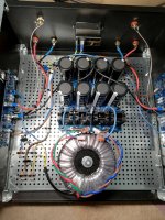
attached pix of actual setting
the only critical thing could be the wires close to the input AC filter connectors to influence some GND oscillations?
or brown (phase) power wire is close to the punched ground plate?
attached pix of actual setting
the only critical thing could be the wires close to the input AC filter connectors to influence some GND oscillations?
or brown (phase) power wire is close to the punched ground plate?
Attachments
Last edited:
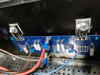
The R9-R12 don't look well soldered. Some part of the weld has to come out to the other side of the PCB. R8 looks very temperature stressed. I had the same in my M2x. Outside the circuit, it measured correctly, but during operation it was extremely hot and distorted the sound. In general, I advise you to improve all welds with tin and flux.
View attachment 936643
View attachment 936643
That channel looks like it's experienced a major event, no doubt.
My thoughts:
1. Don't use heatshrink on the thermistor wires. Heatshrink is extremely soft and is easily punctured, I would switch to teflon or something a little more predictable near hot components
2. Thermistors themselves fully insulated from sink (the washer) and the MOSFET (drain pin) so maybe on the plastic body of the MOSFET.
3. I personally don't like to cross input and output and power supply wires. Cleaning up the layout will help. I would, if possible flip the PCB to have the input at the top, and route the wires for the power supply from the bottom of the chassis. Right now there's a bit of crossing everywhere, not the cleanest of layouts. Flipping the PCB (or sink, which might be simpler?) will also allow easier access to the trimpots, which will now be above everything else.
I don't see any wires for the right channel near the power supply. I would recommend putting in the 1nF optional capacitors.
@darrr
R8 has to be stressed because the MOSfets are gone
R9-R12 are solder with silver solder and yes there was less flux inside, so the solder was not running to the opposite side but there is still a connection
@Atilla
brass parts are 5mm long no action there- thx
@sangram
It seems that I underrate the oscillation possibility of this circuit with this top parts.
What kind of Cap 1nF in feedback path do you recommend ceramic, foil ??
I also will think about the cabling and the RCA input - metal case GND koppling Cap witch I forgot
Also I remember --that in my 3 days of testing i use a prepared RCA plug with shorts the RCA input and as I was connecting the amp to my hifi system the input was OPEN! so an oscillation was possible, I guess.
...stilll not understand why all of it is so touchy and sensitive , due the fact it is according to the schematic and top selected parts...
my prototype with 1058/162 lateral is running fine with no setup issues since 2018..
Last edited:
...stilll not understand why all of it is so touchy and sensitive , due the fact it is according to the schematic and top selected parts...
Did you attempt to connect an input with the amplifier running?
no
i guess he write it:
Also I remember --that in my 3 days of testing i use a prepared RCA plug with shorts the RCA input and as I was connecting the amp to my hifi system the input was OPEN! so an oscillation was possible, I guess.
yes i think this start to oscillating your input, especially if you forgot to use a input cap as you had at your other F5 amp.
chris
- Home
- Amplifiers
- Pass Labs
- F5 power amplifier