McMaster-Carr.com
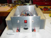
For $125 I have enough for two 12.5"x 13.25" boxes, including 100 4-40 button hex screws w/ shipping. Button heads make the project look nicer IMO!
My heat sinks are 2"x9"x13". ( This is for the mini-ax, not F5. I have other for F5.") )
)
I used a circular saw with carbide blade. Not the best cut, but not horrible either. Some here use a table saw, which is better.
I didn't have a 10" carbide blade for this project.
My brother and friend are machinist. I take it to them to "clean up the cuts" on a mill.
Vince
For $125 I have enough for two 12.5"x 13.25" boxes, including 100 4-40 button hex screws w/ shipping. Button heads make the project look nicer IMO!
My heat sinks are 2"x9"x13". ( This is for the mini-ax, not F5. I have other for F5.
)I used a circular saw with carbide blade. Not the best cut, but not horrible either. Some here use a table saw, which is better.
I didn't have a 10" carbide blade for this project.
My brother and friend are machinist. I take it to them to "clean up the cuts" on a mill.
Vince
EUVL said:Apart from very different Vgs btw P and N devices, the transcoductances also differ by a factor of 1.7 at 2A bias. In comparison to the Toshibas, they are anything but complementary. See attached pdf.
But good. The bias was set at 1.5A per FET at the start, and went up to 2.3A in the end -- quite a bit worst than the Toshiba (1.75A -> 2A) on exactly the same heatsink, etc. Furthermore, the P and the N devices drifted differently with temperature, resulting in an DC offset in the end of something like 25mV. Not that it is an issue, as I am using the balanced version anyway, so they cancel out on both sides.
The frequency response is similar, with a very slight rise of 0.5dB at 600kHz. Probably still curable by fiddling with gate resistor values, etc.
That's interesting. Judging by the results in F5 production, where trimming results in
lowest distortion with a virtually pure 3rd harmonic at 1 watt, the net difference in gain
of the product of JFETs, Drain load, and MOSFET transconductance and Source
resistance is usually within a few percent. The most I have had to trim a Source
resistor is for about a 30% product difference, and that is quite rare.
Interestingly, only a minority of channels require a trim, and the need to trim + vs -
halves is random.
The rest of your numbers are pretty close with regard to temperature drift and DC
offset.
If my measurements are anything to go by, then trimming for even harmonics cancellation does not result in equal gain for both halves, as I thought intially.
It might just be that we have a batch of FETs which have a large difference. As already mentioned in the group buy thread, the variation of Vgs of the P devices are large.
But you are right in a sense. The gain product is within 10% equal with identical Rsource. The factor of 1.7 I was referring to the MOSFETs alone.
What would you suggest to flatten the small hump? Gate resistor to 22R does not seem to do much.
Patrick
> If my measurements are anything to go by, then trimming for even harmonics cancellation does not result in equal gain for both halves, as I thought intially.
A bit of clarification perhaps. I was referring to cancellation of the MOSEFTs alone, ignoring the non-linearity of the JFETs. But this is perhaps good enough as a first order approximation.
At equal gain, the cancellation is about 90% (+/- 5%), which is quite good (factor of 10 reduction in even harmonics). At total cancellation of 2nd, the gain differs by around 15% for the two FETs that I am testing with. But this can vary quite a bit because of Vgs variations and sensitivity of Yfs to temperature.
So I would recommend at least doing the gain balancing if you don't have a distortion analyser.
Patrick
For trim, I simply add parallel resistance to the Source resistor on
either the P or N channel outputs while measuring the distortion at 1
watt, 1 KHz. At some value, the 2nd harmonic essentially disappears,
and there you are.
If your distortion is .01% or so, then trimming will get you down to
.001% to .003%.
Not that I consider this important.
either the P or N channel outputs while measuring the distortion at 1
watt, 1 KHz. At some value, the 2nd harmonic essentially disappears,
and there you are.
If your distortion is .01% or so, then trimming will get you down to
.001% to .003%.
Not that I consider this important.
EUVL said:What would you suggest to flatten the small hump?
What hump is that?
Looking at Patricks measurement of the Fairchilds I wonder why you never bothered to use something more complementary, as the Toshiba 2SK1530?
I guess you simply don't consider the difference worthwile - at least compared to the hassle of getting the more exotic parts
Have fun, Hannes
I guess you simply don't consider the difference worthwile - at least compared to the hassle of getting the more exotic parts
Have fun, Hannes
I have done more analyses today, using 4 different pairs of FETs. The 4 N-FETs have Vgs to 10mV, and the P’s to 20mV.
Taking into account the entire open loop, included the JFETs, and using identical source resistors (0R22 in my case), the open loop gains for positive and negative halves are identical to within +/-5%, and the THD is near minimum (around 0.003% at 1W, 8ohm), but the second harmonics is not zero. If I zero the second harmonics using the MOSFET source resistor, the open loop gains differs by some 10%, and the third harmonics increases, THD coming to around 0.006%. I believe that jackinnj also had the same observation.
So indeed, by balancing open loop gain, you can get good distortion cancellation, despite the largely different characteristics of the Fairchilds.
I have so far detail tested some 20 of each of P and N types, with 16V Vds and DC bias of 2A. Typically, a P-FET would have a Vgs in the order of 5.7V and a transconductance of 3.6S, whereas an N-FET typically measures at 3.6V Vgs and 6.2S transconductance. As already mentioned in an earlier post, the transconductances of the JFETs are also different. This has also to be taken account in determining the open loop gain of each half of the circuit.
The best way to optimise for minimum distortion is, as described by Nelson, to run the circuit up to steady state under actual operating conditions, and adjust the value of one of the MOSFET source resistors, until distortion is minimal.
But then not everyone owns a distortion meter that will measure to better than 0.003%. Nevertheless, distortion cancellation can still be had by balancing the total open loop gain of the positive rail side (N-JFET + P-MOSFET) to that of the negative rail side (P-JFET + N-MOSFET). This can be implemented relatively easily, as follows.
One way of doing this is of course to measure Vgs and transconductances of all devices used under operating conditions (Vgs, Vds, bias, temperature, ….). The attached Excel sheet would then allow you to calculate the loop gain of each side of Ground. And you can either change FET Vgs, or source resistors, or both, to get equal gain.
However, the device parameters, especially transconductance, are VERY sensitive to temperature. Even worse, 2 devices of the same type may even have quite different temperature coefficients. It is amazing to see this happening as you power up two P-FETs, for example, mounted on the same heat sink closed to each other, with the same Vds and initial DC bias, and watching how both bias currents change totally differently as the heat sink warms up.
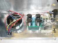
Another, arguably better, way is to measure directly on the circuit board, on heat sink, in housing, under normal operating conditions. The simplest way to measure open loop gain is to disconnect the drain of both MOSFETs from the rest of the circuit, connect them individually each to a 1R 25W resistor (mounted on same heat sink and matched to better than 1%), the other side of which is connected to ground. Apply a 0.01V, 50Hz sine wave to the input using a functions generator (or sound card), and measure the voltage across each of the 1R resistors using either an oscilloscope, or an AC voltmeter (make sure it is DC decoupled). Reduce the value of the MOSFET source resistor on the side having the lower AC output voltage by soldering, say, a 2ohm 1W resistor in parallel with the original source resistor. You would also need to readjust the trimpot at the drain of the JFET to set the bias back to the original value. Repeat the procedure until you obtain equal AC output voltage on each half. Now the open loop gains are balanced, and you can solder the MOSFET drains back to the rest of the circuit. You might also need to readjust the trimpot again afterwards for proper bias and zero DC output voltage.
In my particular case, I drilled the hole on the PCB for the MOSFET drain pin 0.5mm larger than required. Then I applied a short length of thin-walled heatshrink onto the drain pin, where it goes through the PCB. After gain balancing as described, I removed the heatshrink and soldered the drain pin back on the PCB. Cannot be simpler.
Patrick
Taking into account the entire open loop, included the JFETs, and using identical source resistors (0R22 in my case), the open loop gains for positive and negative halves are identical to within +/-5%, and the THD is near minimum (around 0.003% at 1W, 8ohm), but the second harmonics is not zero. If I zero the second harmonics using the MOSFET source resistor, the open loop gains differs by some 10%, and the third harmonics increases, THD coming to around 0.006%. I believe that jackinnj also had the same observation.
So indeed, by balancing open loop gain, you can get good distortion cancellation, despite the largely different characteristics of the Fairchilds.
I have so far detail tested some 20 of each of P and N types, with 16V Vds and DC bias of 2A. Typically, a P-FET would have a Vgs in the order of 5.7V and a transconductance of 3.6S, whereas an N-FET typically measures at 3.6V Vgs and 6.2S transconductance. As already mentioned in an earlier post, the transconductances of the JFETs are also different. This has also to be taken account in determining the open loop gain of each half of the circuit.
The best way to optimise for minimum distortion is, as described by Nelson, to run the circuit up to steady state under actual operating conditions, and adjust the value of one of the MOSFET source resistors, until distortion is minimal.
But then not everyone owns a distortion meter that will measure to better than 0.003%. Nevertheless, distortion cancellation can still be had by balancing the total open loop gain of the positive rail side (N-JFET + P-MOSFET) to that of the negative rail side (P-JFET + N-MOSFET). This can be implemented relatively easily, as follows.
One way of doing this is of course to measure Vgs and transconductances of all devices used under operating conditions (Vgs, Vds, bias, temperature, ….). The attached Excel sheet would then allow you to calculate the loop gain of each side of Ground. And you can either change FET Vgs, or source resistors, or both, to get equal gain.
However, the device parameters, especially transconductance, are VERY sensitive to temperature. Even worse, 2 devices of the same type may even have quite different temperature coefficients. It is amazing to see this happening as you power up two P-FETs, for example, mounted on the same heat sink closed to each other, with the same Vds and initial DC bias, and watching how both bias currents change totally differently as the heat sink warms up.
Another, arguably better, way is to measure directly on the circuit board, on heat sink, in housing, under normal operating conditions. The simplest way to measure open loop gain is to disconnect the drain of both MOSFETs from the rest of the circuit, connect them individually each to a 1R 25W resistor (mounted on same heat sink and matched to better than 1%), the other side of which is connected to ground. Apply a 0.01V, 50Hz sine wave to the input using a functions generator (or sound card), and measure the voltage across each of the 1R resistors using either an oscilloscope, or an AC voltmeter (make sure it is DC decoupled). Reduce the value of the MOSFET source resistor on the side having the lower AC output voltage by soldering, say, a 2ohm 1W resistor in parallel with the original source resistor. You would also need to readjust the trimpot at the drain of the JFET to set the bias back to the original value. Repeat the procedure until you obtain equal AC output voltage on each half. Now the open loop gains are balanced, and you can solder the MOSFET drains back to the rest of the circuit. You might also need to readjust the trimpot again afterwards for proper bias and zero DC output voltage.
In my particular case, I drilled the hole on the PCB for the MOSFET drain pin 0.5mm larger than required. Then I applied a short length of thin-walled heatshrink onto the drain pin, where it goes through the PCB. After gain balancing as described, I removed the heatshrink and soldered the drain pin back on the PCB. Cannot be simpler.
Patrick
Attachments

> I'm now completely confused: are your findings for the stock F5? I thought you build only balanced?
I do.
The gain balancing refers to one half of the balanced circuit, with the intersection point of the X in the latter grounded.
a) There are folks who want to build only single ended.
b) Even for the balanced version, there is no harm to get some distortion cancellation on each half first.
Having said that, the strategy for the balanced version is different from the single ended. In the latter case, you might want minimum THD, or maybe minimum 2nd. In the former case, you don't care so much about even harmonics, as long as they are equal on both sides (left & right), but you might want to minimise the odd harmonics instead.
Patrick
chrismercurio said:I bought mine from Mouser.
Part number: 71-RS02BR4700FE12
Sorry. These were Vishay, not Panasonic.
EUVL said:In the former case, you don't care so much about even harmonics, as long as they are equal on both sides (left & right), but you might want to minimise the odd harmonics instead.
I believe I have mentioned previously that one of the strategies involves
cancellation of 3rd harmonics as well if you can play off the "compressive"
vs "expansive" 3rd.
The transconductance of push-pull fets is expansive with respect to increased
current and voltage and compressive with decrease voltage and current.
Generally, current is increasing with decreased voltage, and vice versa, and
you can look for a load line that minimizes 3rd.
- Home
- Amplifiers
- Pass Labs
- F5 power amplifier