Yep, my typo, it's gate in and drain out so it's common source.
Doesn't mean that it will behave as a common source amp, imo, because both the voltage rail as the 0.47R are connected at the source.
For charging/discharging of the gate, the F5 output stage will behave like a source follower setup imo, Cgd needs to be charged but not Cgs.
If the output stage of the F5 behaved like a regular common source amp there would be a huge problem due to the Miller effect.
6mA would never be enough to charge the gates of the output stage fast enough if the input capacitances would be in the order of several 100pF each, NP clocked the F5 at 1MHz.
Last edited:
Its my understanding that the possible current draw will be less at a certain elevated case temperature
Would mean that any possible higher current demand on the Jfet would be improved if run less hard, in terms of voltage
Seems logical, but not sure it is
cascode
If it results in Jfet running low and in classAB, and cascode pulling the load, Im not sure that will be good
Thats my concern about the cascode at the moment
That Jfet on its own will run too hot or too cool with cascode
If various designs are not working optimal, it wont be fair to do any comparison
We know the same goes fore implementing a unit in a setup
Regarding laterals
At the moment my concern is about the gate resistors
They are usually bigger with laterals, it seems
Some designs use bigger than others
Seems some will even use asymmetrical values on each side, due to asymmetrical transconductanse, which are more equal on the verticals
It might be important to find the optimal values here
Nelson said it might be worth a try, but also indicated that it might need some work
Which means no design changes as such
But obviously not just to throw the laterals in using original values either
I still dont know enough to understand, so it just some thoughts
Last edited:
just trow them in , and follow biasing procedure .
instead of one IRF(P) pair - it's wise to use at least two pairs of laterals , because of xconductance ( lacking in laterals) .
all these questions are beaten to death in this thread ..... twice or trice .....
make it more fun - make two F5s with one supply - one with verticals , one with laterals; connect one to PSU and listen ..... change to other one and listen
use same gate stoppers for both iterations - varying them +/-50% you'll not hear difference .
Right
Even though I do have quads, I also like the idea to have spare pairs, fore an easy repair job, another very nice thing about F5
I expect to use double pairs "only", and standard rails with raised bias
I like to face an easy repair job, if accident happens
A huge advantage I want to hold on to, at almost any cost
Many other amps may just have to be trashed
Last edited:
Polishing
Hey Westend,
That's fantastic. I have to try your technique. Sanding and polishing my Aleph case by hand, it took me days and days and one final day of vowing never to attempt this again!
I have a random orbital sander. But that takes circular velcro 6" sheets and they are relatively expensive. I'll have to look into a palm sander.
Thanks again - nice work and great info,
Steve
Hey Steve,
The polishing process is as follows: Wet sand with 1/4 sheet palm sander-220,320,400,600,800,1000,1500,2000. Buff with rotary 6" car buffer (low speed) No. 7 rubbing compound, Turtle Wax`Polishing Compound for final buff.
Even with an aluminum panel with deep mill marks this process is not that daunting. I only sanded with each grit for a couple of minutes, using different directions. There are better metal polishing compounds but I used what I had on hand.
Hey Westend,
That's fantastic. I have to try your technique. Sanding and polishing my Aleph case by hand, it took me days and days and one final day of vowing never to attempt this again!
I have a random orbital sander. But that takes circular velcro 6" sheets and they are relatively expensive. I'll have to look into a palm sander.
Thanks again - nice work and great info,
Steve
6mA would never be enough to charge the gates of the output stage fast enough if the input capacitances would be in the order of several 100pF each, NP clocked the F5 at 1MHz.
I am not sure what you are saying here. The standard F5 using a single pair of IR devices has an input capacitance of around 1300pF at the gates of the mosfets.
You can't just compare the capacitances and think you have
the whole picture. Input capacitance of the vertical Mosfets
is higher, but so is the transconductance and the result is
that the Gate current at high frequencies is not proportional
to the capacitance figure.
In any case, there is plenty of bandwidth to go around, and
the worst you have to do is use some compensation capacitance
on the feedback loop.
I am not sure what you are saying here. The standard F5 using a single pair of IR devices has an input capacitance of around 1300pF at the gates of the mosfets.
The 1300pF you mention is Ciss.
Ciss is Cgs + Cgd.
When the voltage at the gate of the output devices changes, the voltage at the source of the devices changes in the same amount.
Or, the voltage from gate to rail changes in the same amount as the voltage across the 0.47R resistor.
Cgs is the capacitance between Gate and Source.
If the voltage at the Source "lead" goes up by the same amount as the voltage at the Gate side, then there's NO net charge flowing in or out of Cgs.
Which means that Cgs is not charged/discharged in the F5 output stage layout.
That means that Ciss = 1300pF need not be charged/discharged, but Ciss -Cgs, which is Cgd.
And not all of the datasheet Cgd, but a portion of it.
If you take the word Source in it's meaning as "Origin", then the voltage at the S-lead of the power MOSFET follows the Source=> Source Follower.
Papa says that MOSFETs don't know which is up and what is down, just where it goes in and where it goes out.
Well, something like that in prettier words.
Last edited:
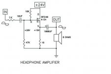
Somewhat off topic Headphone amp in service manual
I decided to build the headphone amp from the service manual, since the parts are minimal. It works just dandy, however the 50 watts of resistors making my 16ohm source resistor still run about 120c. The heatsink for the mosfet runs cool. Any idea what the ideal resistor wattage is here? Looks like a heatsink type for sure...
I decided to build the headphone amp from the service manual, since the parts are minimal. It works just dandy, however the 50 watts of resistors making my 16ohm source resistor still run about 120c. The heatsink for the mosfet runs cool. Any idea what the ideal resistor wattage is here? Looks like a heatsink type for sure...
Attachments
I've replaced the one channel that burned out. I made sure my soldering was very good.
Every thing seemed great. Then the newly installed channel was starting to have distortion. I check the dc offset on the terminals and it was all the way up to 500mV!
The resistors on R11 and R12 were very low, under 30mV. I've hit a wall. This situation is very similar to before, when the same channel burned out when I messing with the pots trying to correct the problem. All new parts and pcb were installed. I would really appreciate any help.
Last edited:
Your resistor should dissipate 16 watts only.
Did you measure 16 volts across it?
The measurements are exact to what's posted. Someone did their homework.
The 16 ohm resistor from source to ground just seems to need a be a large power resistor.
The measurements are exact to what's posted. Someone did their homework.
The 16 ohm resistor from source to ground just seems to need a be a large power resistor.
The 16 ohm resistor needs to be a power resistor, just as Nelson writes it in the text. Pity though he didn't specify a Watts rating for it. Nelson, could you shed some light onto this matter?
Just work it out
And for driving a pair of headphones that IMO is obscene, but there we go.
I was hoping for some help there.
I have 45 watts of sand-cast wirewounds bundled together, putting off an enourmous amount of heat. a Finned heatsink mountable seems the way to go, but what wattage? Right now just a little clip lead project to get an idea of the sound of the unit.
- Home
- Amplifiers
- Pass Labs
- F5 power amplifier