f5 w/Parallel Output IC
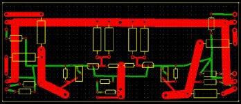
I am trying to create my own pcb for the first time and I would appreciate any and all advice or critique of the attached layout. I am laying out a board for an F5 with parallel output trans and no limiting circuit.
I am using free software from express PCB, but is there a better inexpensive program.
Cheers Nick
Attachments
I use this
http://www.abacom-online.de/uk/html/sprint-layout.html
40 Euros for a download. Its very easy and exports gerbers. Its not the best but it is probably the best low cost (read 'not free') that I know of for a total beginner. I have made many boards with it with ease.
Here is a list of many free and open source programs.
It mentions mine but the shortcoming it mentions has been fixed.
http://www.olimex.com/pcb/dtools.html
Uriah
Re: f5 w/Parallel Output IC
When considering a layout, the run from the drain of the JFET's to the gate-stopper resistors, and the run to the MOSFET gates from these resistors should be as short as possible.
npapp said:I am trying to create my own pcb for the first time and I would appreciate any and all advice or critique of the attached layout. I am laying out a board for an F5 with parallel output trans and no limiting circuit.
I am using free software from express PCB, but is there a better inexpensive program.
Cheers Nick
When considering a layout, the run from the drain of the JFET's to the gate-stopper resistors, and the run to the MOSFET gates from these resistors should be as short as possible.
Jack, thanks for that tip
However if I was using stripboard, I'd need to connect Q5, R3, R15 and P1 to the junction of Q1 and R13 (I'm assuming short connections are required here too, if they are not it makes life a little simpler). This automatically makes it a pretty long trace (5 -6 holes on a stripboard, the pot will take 2-3). The second condition is more easily fulfilled, I can probably solder R13 directly to the gate.
However if I was using stripboard, I'd need to connect Q5, R3, R15 and P1 to the junction of Q1 and R13 (I'm assuming short connections are required here too, if they are not it makes life a little simpler). This automatically makes it a pretty long trace (5 -6 holes on a stripboard, the pot will take 2-3). The second condition is more easily fulfilled, I can probably solder R13 directly to the gate.
Re: Re: f5 w/Parallel Output IC
This does not seem to be the case here
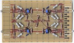
http://www.6moons.com/audioreviews/firstwatt7/f5_2.html
jackinnj said:
the run from the drain of the JFET's to the gate-stopper resistors ... should be as short as possible.
This does not seem to be the case here
http://www.6moons.com/audioreviews/firstwatt7/f5_2.html
Re: Re: f5 w/Parallel Output IC
Thanks for the advice. Which side of this is most critical, the jfet to gate-stopper or gate-stopper to MOSFET? I think I will most likely only be able to accomplish one side of this recommendation since I am hoping to distribute the MOSFETs further apart on the heatsink.
jackinnj said:
When considering a layout, the run from the drain of the JFET's to the gate-stopper resistors, and the run to the MOSFET gates from these resistors should be as short as possible.
Thanks for the advice. Which side of this is most critical, the jfet to gate-stopper or gate-stopper to MOSFET? I think I will most likely only be able to accomplish one side of this recommendation since I am hoping to distribute the MOSFETs further apart on the heatsink.
Re: Re: Re: f5 w/Parallel Output IC
I will stick to my story. The gate resistor on the MOSFET should be as close as possible to the output device. I can get my F5's to operate into the MHz without problems (yeah, I know that's an abusrdity).
bobodioulasso said:
I will stick to my story. The gate resistor on the MOSFET should be as close as possible to the output device. I can get my F5's to operate into the MHz without problems (yeah, I know that's an abusrdity).
Re: Re: Re: Re: f5 w/Parallel Output IC
No, it's not - since you try to check & proof the stability of your amp!")
Cheers,
jackinnj said:
I can get my F5's to operate into the MHz without problems (yeah, I know that's an abusrdity).
No, it's not - since you try to check & proof the stability of your amp!
Cheers,
Re: Re: Re: Re: f5 w/Parallel Output IC
I totally agree with you but you spoke also about the distance from JFets to this resistor, which doesn't look so important to me.
Though i may be wrong as i did not experiment with this.
jackinnj said:...The gate resistor on the MOSFET should be as close as possible to the output device...
I totally agree with you but you spoke also about the distance from JFets to this resistor, which doesn't look so important to me.
Though i may be wrong as i did not experiment with this.
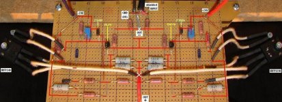
I have a run of 0.300 inch (7.6mm) from gate-stopper to mosfet. The F5 layout shown on 6-moons spreads the MOSFET's heat better. Still I have 4 of these guys running -- from mounting hole to mounting hole the spread is 3.800" = 96.5mm and eyeballing the First Watt amp it would appear to be 2x this at least.
Jack, what about the other end? I can probably get within a few millimeters myself on the gate side, but will be difficult on the drain of Q1. There are at least 4 solder connections to be made on that 'track', and this will make it really tough to get better than 15mm or so, maybe a bit more.
I can definitely get shorter traces from the jfet drain to the g-s resistors if I move the jfet further toward the MOSFETs, but this gives me a much longer input trace from R1 to the jfet source. Should I worry about the input trace length? I was trying to keep it as short as possible.
N
N
npapp said:I can definitely get shorter traces from the jfet drain to the g-s resistors if I move the jfet further toward the MOSFETs, but this gives me a much longer input trace from R1 to the jfet source. Should I worry about the input trace length? I was trying to keep it as short as possible.
I wouldn't lose any sleep over it.

- Home
- Amplifiers
- Pass Labs
- F5 power amplifier