Hi Housing,
Thanks for pointing out to the LM340 pinout. Checked the data sheets, and you are correct, the pinouts are different. My bad. The LM317 pinout is the same but output noise is the same and ripple rejection only slightly better. Probably not worth changing, unless someone has a suggestion for a better part. Pity that Spencer threw the 7805's overboard in this case as they are a better part than the LT replacement. I suspect Mr. Colburn had a clue or two about parts selection.
In regards to parallel zeners, you read should the link on 3pin regs above for reasoning on use of parallel zeners. The argument is that paralleling halves the impedance of the zener. It certainly seems to work ok, and has been widely used in the "raygulator" discussed in the "Marantz CD63 & CD67 mods list" thread.
As a side note, the output impedance of the LM3x7's of the could be further improved by separating the adjust pin gnd and load gnd as described by Werner Ogiers. I can't see how this can be done easily with the current board.
http://www.tnt-audio.com/clinica/regulators2_impedance1_e.html
cheers
Paul
Dave said:Spencer,
I think the 47uH inductors you have inline with the PCM63 supply rails might be a concern. These will form a resonant circuit with the 47uF capacitors, resonant frequency will be 3.386kHz right in the audio band.
The characteristic impedance is 1 ohm so the DC resistance of the inductor and/or ESR of the cap might be enough to damp it properly but could be worth double checking.
Dave
Hi Dave
So this resonance would show up as an oscillation on the V+/V- lines? How would we test for this phenomena?
cheers
Paul
spzzzzkt,
The resonance could lead to very poor transient response on the output of the filter. When the load current steps up the output voltage will drop and ring if the damping is not enough. Perhaps more of a concern is if the load current steps down, in this case the output of the filter will overshoot as energy that was in the inductor is transfered to the capacitor, if the overshoot voltage is enough it could destroy the load. Again there is the potential for ringing. Best bet is to ensure that the filter is properly damped. Play with it in a spice simulator.
Dave
spzzzzkt said:Looks like the LT1117's stay for the moment then")
Will Burr Brown's Reg1117A-5 be better sounded although their specifications are almost the same except that the Reg has a current output of 1A?

ctong said:Can the IV and output stages be used with DACs accepting DSD signals such as PCM1738 and PCM1792? These DACs are Sigma-Delta type for PCM signals.
There is a thread dealing with D1 I/V and the PCM1738:
http://www.diyaudio.com/forums/showthread.php?s=&threadid=31732
housing said:
Will Burr Brown's Reg1117A-5 be better sounded although their specifications are almost the same except that the Reg has a current output of 1A?
I think that question can only be answered by listening tests not spec racing. Maybe Spencer had some specific reason for choosing the LT part?
My choice of regulator is less aggressive regulator (less internal feedback) like standard LM317, LM337 from ST and also LT1117-5V from ST. I feel the sound from LT regulators are a bit harsh.
Playing with the power supply decouple capacitors next to the analogy supply of DAC chips and the Jfet IV is also fun and so far the Pana FC cap give very good and non harsh sound. I think there is better cap like Pana FM or even black gate etc... but it all depends on how much you want to spend.
For output couple capacitors, the Black Gate N 10uf 50V sound very good also and it do not require any shielding.
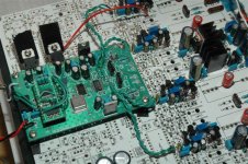
I have tried the PCM1798 on the Jfet IV section as output stage and is all working fine. The current source at top and bottom need to be adjusted properly.
Playing with the power supply decouple capacitors next to the analogy supply of DAC chips and the Jfet IV is also fun and so far the Pana FC cap give very good and non harsh sound. I think there is better cap like Pana FM or even black gate etc... but it all depends on how much you want to spend.
For output couple capacitors, the Black Gate N 10uf 50V sound very good also and it do not require any shielding.
I have tried the PCM1798 on the Jfet IV section as output stage and is all working fine. The current source at top and bottom need to be adjusted properly.
Attachments
Hi Spencer,
I've been meaning to ask what you felt the advantages of the JFET I/V was over MOSFET. I noticed you have built both versions so thought you might have some ideas.
I've read something recently that suggests in the D1 I/V converter the input resistance/transconductance of the transistors is the most important factor and that the original MOSFETs may actually be better in this situation than using J/FETs.
cheers
Paul
Paul,
It is base on listen preference and I like the Jfet IV more. I get more life in the music if I use Jfet. The transconductance of K170 is 20mS and thus the input impedance is about 1/20ms = 50 ohm. If you parallel two K170, you get a bit lower input impedance but I prefer the sound of single K170. Of course you can use other Jfet or parallel more. Moreover you can bias the K170 at different current and select your sonic preference.
Spencer
Spencer,
Thanks for explaning. I'm tempted to put a MOSFET I/V together anyway - just to see how it sounds compared with the jfet version
Mo' Zener Fun
I've also redone the DAC 317/337 zener mod with 3V 0.4W zeners and 1N4148. The 1W zeners I used originally were massively over rated and the paired 0.4W zeners fit far better, taking barely any more room than the resistors they replace. Supplies are now sitting close to 4.9V so there is a little more safety margin than the previous worst case 5.45V.
I clearly wasn't paying attention, as I didn't realise the 12V supply is smoothed but not regulated. I was wondering what was wrong when I stuck a probe on the +12 and saw the ripple. I'm tempted to rewire so the DAC regs are powered from the 18V analog supply.
Even with the current setup the zener modded DAC regulators have improved detail. The addition of on the zeners to the analog have made another small improvement to detail. I'm sure adding a 10uF bypass from adj to gnd on the 3*7's will clean the supplies up a bit more so that is the obvious next step.
cheers
Paul
Thanks for explaning. I'm tempted to put a MOSFET I/V together anyway - just to see how it sounds compared with the jfet version
Mo' Zener Fun
I've also redone the DAC 317/337 zener mod with 3V 0.4W zeners and 1N4148. The 1W zeners I used originally were massively over rated and the paired 0.4W zeners fit far better, taking barely any more room than the resistors they replace. Supplies are now sitting close to 4.9V so there is a little more safety margin than the previous worst case 5.45V.
I clearly wasn't paying attention, as I didn't realise the 12V supply is smoothed but not regulated. I was wondering what was wrong when I stuck a probe on the +12 and saw the ripple.
I'm tempted to rewire so the DAC regs are powered from the 18V analog supply.Even with the current setup the zener modded DAC regulators have improved detail. The addition of on the zeners to the analog have made another small improvement to detail. I'm sure adding a 10uF bypass from adj to gnd on the 3*7's will clean the supplies up a bit more so that is the obvious next step.
cheers
Paul
The truth about LT1117
Found this little nugget in the LT1117 data sheet:
so we have: output noise voltage of 150uV and ripple rejection of 63dB (typ)/47dB(min).
figures like these make a 7805 look high performance!!
Another tidbit found surfing the datasheets was that for 5V applications 25uF is recommended for the 3x7 adj pin bypass cap. The lower ESR of the 25uf cap (vs 10uF) is apparently required to compensate for the small value of the adj resistor (300R in this case). The addition of the adj bypass improves ripple rejection very significantly ( about 15dB), so I would not consider this to be an optional tweak - more like a basic requirement for good performance from the 3x7 regs.
Found this little nugget in the LT1117 data sheet:
For fixed voltage devices, and adjustable devices without
an adjust pin capacitor, the output ripple will increase as
the ratio of the output voltage to the reference voltage
(VOUT/VREF). For example, with the output voltage equal to
5V, the output ripple will be increased by the ratio of
5V/1.25V. It will increase by a factor of four. Ripple
rejection will be degraded by 12dB from the value shown
on the curve.
so we have: output noise voltage of 150uV and ripple rejection of 63dB (typ)/47dB(min).
figures like these make a 7805 look high performance!!
Another tidbit found surfing the datasheets was that for 5V applications 25uF is recommended for the 3x7 adj pin bypass cap. The lower ESR of the 25uf cap (vs 10uF) is apparently required to compensate for the small value of the adj resistor (300R in this case). The addition of the adj bypass improves ripple rejection very significantly ( about 15dB), so I would not consider this to be an optional tweak - more like a basic requirement for good performance from the 3x7 regs.
Housing,
Look closer at that spec for output noise: it is 10uV/V*Vout so actually 50uV for 5V output. RR is 65dB.
7805 still looks better on paper. 40uV output noise and 80dB (typ.)/62dB (min) RR...
BTW I've ordered a board for Tangent's LNMP http://www.tangentsoft.net/elec/lnmp/, so once I get that up running I'll have a far better idea of what's happening on the supplies in terms of noise and what difference the tweaking is making.
I want to build/test a D1 78xx supply once I've got the preamp for my scope. I'm interested to see how it performs.
cheers
Paul
Take note on the following points:
1. Lower noise is always better. I use two steps series regulators for both digital and analogy supply. But the digital part generates too much noises from each chip. The noise source is from the chip, not mainly from the transformer.
2. Changing to different regulator (series, shunt, part number, different manufacturer etc) chip will also change the sonic. Note that the output impedance, CMRR, noise spectrum, speed etc of different regulators will be always different (LT, LM, 78/79 series). Experiment and choose the one that suit your sonic taste. I think Pass always use a simple series non feedback regualtor will be his preference of the type of sonic from this kind of regulator.
3. In my D1V3 board, I did not put the decouple cap at the 317/337 ground resistors due to lack of space, you can always solder one at the bottom of the pcb as you like.
Enjoy tweaking!
VCXO Reclocker
I think I have finally worked the purpose of the bias voltage in the secondary PLL. I came across a couple of texts discussing jitter caused by the dead band on the 74HC4046 phase comparator. I found a passage in ch. 10 of the ARRL handbook which mentioned that it was common to bias the PLL to force the comparator to operate outside the dead band as a means of reducing jitter.
So it would seem that it's worth implementing the bias portion of the circuit, tho it will most likely require tweaking for use with a different VCXO.
SMD soldering
Hi,
I have just read the SMD soldering guide here http://www.infidigm.net/articles/solder/
and the "flood and suck" method is rubbish.
Also no where on that page does it mention the use of flux!!! Which is the key ingredient when soldering fine pitch surface mount ICs.
What you want to do when soldering surface mount ICs is,
place part on PCB and line up over the pads.
solder down one pin at say the corner, this is the hardest bit as you need to keep the device in position when doing this. However don't worry if you bridge to the next pin.
solder down another pin at a corner.
apply flux (i use kester #186 RMA flux pens, digi-key KE1803-ND) all over all the pins.
apply a small amount of solder to the tip of a soldering iron.
drag this down a row of pins.
if you put the right amount of solder in the iron it will solder all the pins perfectly and it is actually quite hard to bridge pins!
This is all actually pretty easy, I can solder 100 pin QFP packages with 0.5mm pin pitch easily.
Also when soldering DAC chips too much heat will throw off the trimming of the internal resistors. This will increase distortion a great deal but the part will still work. I would say the "flood and suck" method will almost certianly do this.
Dave
- Status
- This old topic is closed. If you want to reopen this topic, contact a moderator using the "Report Post" button.
- Home
- Amplifiers
- Pass Labs
- Pass D1V3 DAC - build thread