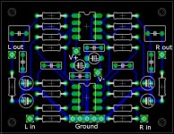
I'm trying to make a RIAA preamp based on this schematic. I have now a decent version which I'd like you to comment on. A few pointers:
1. All the ground connections are on the bottom row: L input GND, L output GND, power supply GND, R output GND and R input GND. (The turntable earth will also have a connection there - now it is missing).
2. There is no star ground implemented but all the ground points are very close to each other and the tracks are not too narrow (GND track width is 45mil.) AFAIK this should minimize/eliminate all the troubles any voltage differences might produce.
3. Signal track width is 20mil.
4. You can see 4 bypass capacitors very near op-amp (NE5532) supply pins. There are 10uF and 100nF caps there for both rails. First I though of only having 100nF but then I found a way to fit those electrolytics there.
5. The design is as symmetric as possible.
6. The board size is 2.4" x 1.85".
Any comments or suggestions are welcome!
Attachments
Thanks for the comments!
I think that the center is the best placement as there are two supply pins on both op-amps. If I move a cap to one end the distance to the other supply pin grows way too large. In the center the distance is about equal to both op-amps.
Is that really needed? In the project page it is recommended to have one 100nF and one 10uF "for each supply line" not for each op-amp. And this seems to be the case in the PCB picture there. Not sure though. I'm very new to this but this is what I have gathered:
So based on this info I see no need for 4 more components in this layout. (The situation could be different if the board was larger, had way more op-amps, operated at higher freq. But please correct me if my assumptions are not valid.
PS. I really should get that "Art of Electronics" by Horoqitz&Hill...


BrianDonegan said:I would move the 0.1uF films to the opposite ends of the op-amps. You wan them as close to the power pins as possible.
I think that the center is the best placement as there are two supply pins on both op-amps. If I move a cap to one end the distance to the other supply pin grows way too large. In the center the distance is about equal to both op-amps.
Nordic said:Yeah, and add 2 more... 1 for each power pin...
Is that really needed? In the project page it is recommended to have one 100nF and one 10uF "for each supply line" not for each op-amp. And this seems to be the case in the PCB picture there. Not sure though. I'm very new to this but this is what I have gathered:
- Oscillation might happen if the input voltage is not truly DC.
- Bypass caps filter the AC component from the voltage.
- We need different values because of capacitor self resonant frequency -> small value caps have usually lower impedance at high frequencies.
- The voltage potential should be identical in all points between the supply pins of the two op-amps.
So based on this info I see no need for 4 more components in this layout. (The situation could be different if the board was larger, had way more op-amps, operated at higher freq. But please correct me if my assumptions are not valid.
PS. I really should get that "Art of Electronics" by Horoqitz&Hill...
- Status
- This old topic is closed. If you want to reopen this topic, contact a moderator using the "Report Post" button.