Here is design which came from a french review LED which did not exist anymore. The author is J.Gest, but the second part of the article has never been published.
The bad thing is that I have started this project, bying all the parts... I've try different ways to make a pcb layout but the result is desastrous.
Could comeone here help me for this?
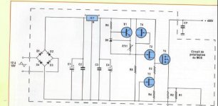
Here is the component list and the logical diagram. And sorry guys in the thread "CCS for tubes/valves: PCBs" where I start posting this, looks like it was the wrong place")
R1=12 Ω 1/2W
R2=12 Ω 1/2W
R3, R4=33Ω 1/8W 5% if T2 and T3 2SK170BL
R3, R4=22Ω 1/8W 5% if T2 and T3 2SK170GR
R5=330 Ω 1/4W 1%
R6=7.5kΩ 1/2W
Rv1=5 kΩ 10 or 25 turns
C1=220 µF 35V 105°C
C2=220 nF 50V
C3=220 nF 50V
C4=22 µF 35V tantale goutte or CTS13
D1 to D4=1N4007
D5=TL 431
T1=BC549C
T2=2SK170GR or BL
T3=2SK170GR or BL
T4=2SK30AGR
T5=IRF840, IRF840AFI
IC1=7812
Thanks,
The bad thing is that I have started this project, bying all the parts... I've try different ways to make a pcb layout but the result is desastrous.
Could comeone here help me for this?
Here is the component list and the logical diagram. And sorry guys in the thread "CCS for tubes/valves: PCBs" where I start posting this, looks like it was the wrong place
R1=12 Ω 1/2W
R2=12 Ω 1/2W
R3, R4=33Ω 1/8W 5% if T2 and T3 2SK170BL
R3, R4=22Ω 1/8W 5% if T2 and T3 2SK170GR
R5=330 Ω 1/4W 1%
R6=7.5kΩ 1/2W
Rv1=5 kΩ 10 or 25 turns
C1=220 µF 35V 105°C
C2=220 nF 50V
C3=220 nF 50V
C4=22 µF 35V tantale goutte or CTS13
D1 to D4=1N4007
D5=TL 431
T1=BC549C
T2=2SK170GR or BL
T3=2SK170GR or BL
T4=2SK30AGR
T5=IRF840, IRF840AFI
IC1=7812
Thanks,