I am trying to produce a PCB using a film developed from a redrawn pdf file, then PCB goes thru an exposure and developing process and finally the etching. Problem is that the results are far from good. I have posted a pic of how it looks like with holes on the tracks where they should not be. Anyone encountered this using whichever method and would like to share the solution to this problem? 
Thanks.....
An externally hosted image should be here but it was not working when we last tested it.
Thanks.....
Howdy safetyman,
Ooops, several things can be happening.
If you are using a black and white film to UV expose the presensitized board, the time/intensity can be wrong. The film can be not in good physical contact with the board causing bubbles or bits of dust between the two. Or the film may have small holes in the traces not easily seen without a light table. The exposed board can be overdeveloped causing small holes that etch larger. The etching solution can be too strong, temperature high or longer than needed. The presensitized board can have problems of its own. Date of make can be a factor.
If you use a magnifyer over the developed board before etching, you may see the problems first. Then it can be fixed using an oil based ink pen or model airplane enamel paint and a small brush. Neither is much fun, but better than holes in the traces.
You can of course just ignore the holes. Get some good silver solder and completely "tin" the entire board with enough solder to fill the holes.
Try again and standardise every step. Making quality pcb's is a learned craft with a bit of voodoo involved. My first boards were a much bigger disaster.
Guys, thanks the help.
The exposure was done with a unfiltered 2000watt UV lamp for 120 secs. This is actually one of those exposure machines that printers use to make their printing blocks with. My friend is a printer and this is the first for him in making a copper board. I believe their printing blocks are not made out of copper.
That could well be the main culprit.
Hi safetyman,
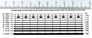
we all make errors and correct them. In order to get better boards, find in the pic a sample containing tracks, numbers and pads. The number above are 1mm height. At the left and at the right of the tracks you see their width (left : mm, right : thou). I have put a ruler in order to let you appreciate the dimensions of the board (in cm).
This pic is difficult to get on the board. The zero may come pqartially or fully filled, the 9 and 0 may not be separate, the tracks may come not evenly etched (variable width), the tiny hole in pads may not appear ... You have so a way to get errors to correct without throwing away precious $ in etching full boards...
I use always this pic and calibeate my process in order to correct the exposition time when I get new boards. When it is calibrated ok, it is ok for all the otyher boards I have got.
Don't overlook the 3 last sentences of acenovelty's reply : they are truth and the way to go. My first boards were awfull too. Yours is much better.
Regards
rephil
Attachments
Thank you, thank you for the guidance.
rephil, thanks though I do not understand what I am supposed to do with the pic? Am I supposed to do a board with that and get the method right till everything shows up and that means that would be the way to go?
Anyway, I did another board exposing it to the same source for 95 secs this time round instead of the 120 secs. After etching, the result us much better, except that some of the "pads" (I think that's what they are called) on the finer tracks were etched off but generally, no holes this time. Another problem that showed up though, is that some of the tracks seem to be scratched. Is this normal? Is there anything that I can do to fix this?
Beside the above circuit, on the same board, I had a preamp circuit with much finer tracks and when that was etched, some of the tracks went missing. Could this be an indication of the solution being too strong?
Thanks again.
rephil, thanks though I do not understand what I am supposed to do with the pic?
Am I supposed to do a board with that and get the method right till everything shows up and that means that would be the way to go?Anyway, I did another board exposing it to the same source for 95 secs this time round instead of the 120 secs. After etching, the result us much better, except that some of the "pads" (I think that's what they are called) on the finer tracks were etched off but generally, no holes this time. Another problem that showed up though, is that some of the tracks seem to be scratched. Is this normal? Is there anything that I can do to fix this?
Beside the above circuit, on the same board, I had a preamp circuit with much finer tracks and when that was etched, some of the tracks went missing. Could this be an indication of the solution being too strong?
Thanks again.
Sounds like underexposure/underdevelopment. But then under exposure and over development causes similar problems at the etch.
What are you using for the etch solution? You can also over etch as in too strong solution, temperature too high or too long in the etch solution. This is where the voodoo comes in as everything must be in balance for a good board.
Keep on trying. You've only made a couple attempts.
Some folks claim better success with a laser printer and Press-N-Peel Blue. http://www.techniks.com/
No developing, but ironing down big boards is a different problem.
ace, I am expreimenting but it's getting pretty expensive with ruined boards. I think the Press-N-Peel Blue is not available where I am and I am trying to master this process as I need to produce about 10 or so boards for my friends and myself to do. The solution used is ferric chlorite.
I'll defnitely update this page as I go along till I find the right process. This way, the page may be useful for some poor soul in the future who faces the same problem as I do.
I think the Press-N-Peel Blue is not available where I am and I am trying to master this process as I need to produce about 10 or so boards for my friends and myself to do. The solution used is ferric chlorite.I'll defnitely update this page as I go along till I find the right process. This way, the page may be useful for some poor soul in the future who faces the same problem as I do.
Fairly certain the folks at technics.com will ship to you.
"Ferric chlorite" from crystals? If so, dissolving in the correct amount of water is important for strength. You can control the etch activity with temperature. Some agitation of the etch solution over the board is required to carry away the etched copper from the board.
The ole guy who showed me called this process "payin' yur dues".
Keep on tryin'. Once you get it, the knowledge lasts a lifetime.
Hi safetyman,
the pic has been drawn using a CAD program (Proteus from Labcenter in UK). The pic has been printed on a transparency suitable to my HP deskjet 5652 (here I use Tartan 707 transparencies). It is printed twice on the same transparency in order to get black 'more black than black'
You should draw such a pic in order to adjust your process.
I cut a board and get a few 10cmX3.5cm small boards from it. Then I do a sandwich with one of the small boards and proceed with the exposure to UV.
Then I proceed as you do with chemicals. I use ammonium (or sodium or potassium) persulfate instead of ferric chloride because it is not colored. This allows me to get simple visual control of the etching process.
2nd part follows.
Regards
rephil
2nd part
Hi safetyman,
I use a small 6X magnifier lens in order to inspect the PCB. If not OK, I do some change in the process and create a new etched small board as before. This until needed.
In order to get info do a google search on : etching pcbs. A lot is available IMO.
A must : download the catalog from www.megauk.co.uk. They are friendly and will cut a big board into smaller one on request. Their DM9001 shear works very fine. A good buy. Don't try to use shears aimed at paper cutting : they can't do it with PCBs.
Take a look at www.electricstuff.co.uk (How to make really good homebrew PCBs) and at www.ladyada.net/resources/inhouseetch.html.
I hope this helps you. Have fun.
Best regards
rephil
Hi,
I think that the exposure time is about right.
WRT the thin horizontal line: this looks like there was too much distance between the film and the resist. The toner should have direct contact to the photo resist.
I usually make such a sandwich: glass plate - bottom film printed normally - double sided board - top layer film printed mirrored - glass plate. Then I execute some pressure between the glass plates by applying lots of duct tape. 6 mil traces are no problem. (HP Laserjet 6 MP, Avery/Zweckform 3491 "laser film for print master production", Bungard presensitized boards)
The glass attenuates the UV light somewhat; you may need the double or even triple exposure time depending on thickness and material. Make a test board whith a strip of film that you move away inch by inch every 30 seconds.
When making double sided boards, I first mount the bottom film on the bottom glass. Then I surround the location of the board proper with old FR4 material on two or 3 sides. On this I mount the top film. It is easy to align top and bottom in the tru light so that the holes meet and the film stays completely flat. This all takes a lot of adhesive tape.
Then I insert the presensitized board into the poach. Got to be careful here not to scratch the toner. Finally, I add the top glass plate and press the stack together.
The voids in the traces of your board seem to have very sharp edges, so they probably do not result from over-exposure. I speculate that your developper has been prepared just before the development process and still contained NaOH pieces.
... and when preparing developper: First the water, then the NaOH. Play it save.
regards, Gerhard
ace, there's so much truth in your wise words and onwards I plod.
rephil, I got what your drift. I'll definitely look at calibrating once I have the chance.
gerhard, the exposure process was done in a machine that sucks the air out of the compartment thus a vacuum b4 the developing process. Don't think the contact is a problem but will check.
Thanks again guys. Out of town now but when I get back, I'll be trying the next round.
And I'll report back.
Thanks for all the suggestions.
Looks to me like you had something splashed on the coated board before exposing it. If these were pre-sensitized boards, they may not have been in good shape. I know of no way to clean them beforehand, but that isn't to say there is no way... just haven't looked into it. The fine lines could be scratches or hair on the mylar pattern or on the board.
I usually look at my boards, then touch up with an indelible marker, a really fine one. I thicken up thin traces and draw circles around pads. Your first board you showed up looked like the right exposure. The etching is critical, though. If etched too long or too strongly, it can eat under the resist.
I've made quite a few using sensitized boards and UV light, but lots of bad ones, too. About 50% yield.
It takes practice, and good materials, clean solutions, known temperatures.
Mike.
PCB ETCHING
Am Going in the same direction with making PCB 'S .When making the transparency for use with positive resist boards which part of the board is exposed to the UV light, the trace portion or the waste portion??? I did this years ago with the old Kepro stuff and I cant remember which part of the transparency was black!!
Am Going in the same direction with making PCB 'S .When making the transparency for use with positive resist boards which part of the board is exposed to the UV light, the trace portion or the waste portion??? I did this years ago with the old Kepro stuff and I cant remember which part of the transparency was black!!
PCB
I had the exact same problem! I swapped to the press 'n' peel option which works very well. You need to make sure the iron is not too hot and don't press hard and this produces some great results?
After all, you can touch up your design with permanant markers.
Good luck,
wotsascott.
I had the exact same problem! I swapped to the press 'n' peel option which works very well. You need to make sure the iron is not too hot and don't press hard and this produces some great results?
After all, you can touch up your design with permanant markers.
Good luck,
wotsascott.
It is is kinda strange to me that you have problems with photo PCB's. I have made hundreds of photo PCB's, and the only trouble I've ever encountered were related to exposure time. When starting out with a new type of board, I usually make a quick test by exposing a couple of small pieces 60 to 120 seconds, develop them and see what went well. Besides that all you need to do is to make sure your development solution is right and pay attention when developing/etching, which is fairly easily done by visual check.
Magura
Magura
press 'n' peel is really the way to go. very precise and a cinch to fix up with a permanent marker, as someone said previously. here are some boards done with pnp, see for yourself
An externally hosted image should be here but it was not working when we last tested it.
An externally hosted image should be here but it was not working when we last tested it.
An externally hosted image should be here but it was not working when we last tested it.
- Status
- This old topic is closed. If you want to reopen this topic, contact a moderator using the "Report Post" button.
- Home
- Design & Build
- Parts
- Problem with etching PCB!!! Please help!