Lately I have been trying to make a PCB for a linear regulator that I designed. The schematic is done and when in Eagle I quickly got it to transfer everything to the board layout for me. The hard part is routing the traces and getting all the components in the right spots. I can't seem to ever get the board layout looking good without wires going everywhere. I ended up getting frustrated and using the autorouter instead. I would like to be able to build a good stable board before I spend money on making one. Do you guys have any tips or tricks to designing and laying out all the components and traces? It would be greatly appreciated!!
Pic of schematic: http://webrocket.ca/schematic.jpg
Pic of board: http://webrocket.ca/board.jpg
Regards,
Chris
Pic of schematic: http://webrocket.ca/schematic.jpg
Pic of board: http://webrocket.ca/board.jpg
Regards,
Chris
Eagle
Hi Triden,
I too was frustrated with Eagle and how it went from schematic to board.
My solution was to create the board directly from the "Board" view and not from the schematic.
Create a new blank (empty) PCB, make it the size you want, and then start adding components to it, moving them around. Slowly start putting in traces and more components.
When you are done with the routing you can change the trace thicknesses and even their layer (top or bottom). its easy to delete and add components as well.
I have never created a board before and was able to get a few boards made using this technique!
Anyway, I don't know if you knew Eagle had this capability, if you know the schematic just place the parts onto a blank board and it was much easier this way for me.
You want to use double layer? With such a simple circuit bottom layer only should be OK.
It looks to me, that you first placed components on the board to make it nice looking. Wrong! Go step by step, place them on board one by one, rotate devices when needed, change positions.. optimizing is kind of trials and errors algorythm")
Look at schematic, no wires are crossed, this is a good startng point to start designing PCB.
And use thicker traces!!
cheers
It looks to me, that you first placed components on the board to make it nice looking. Wrong! Go step by step, place them on board one by one, rotate devices when needed, change positions.. optimizing is kind of trials and errors algorythm
Look at schematic, no wires are crossed, this is a good startng point to start designing PCB.
And use thicker traces!!
cheers
Alright, I will try the technique of slowly adding devices 1 by 1. Does it matter if I choose to do it on a single side as oppose to 2 sides? Also, how do you know how wide the traces will be? The board will put out 1.5Amps max at 25vdc. I don't understand Eagles measurments of "MIL".
Now I want to be able to put wires through the pads that I made. Its about 18 guage wire...but how wide do I made the hole. Are there any references for these?
Thanks,
Chris
Now I want to be able to put wires through the pads that I made. Its about 18 guage wire...but how wide do I made the hole. Are there any references for these?
Thanks,
Chris
Eagle
Holes are actually a component- add them, they are in libary "holes."
to change a line width, draw the line as you normally do, then click the wrench ("change") go to "width" and select a bigger value, click on a trace and the trace will get bigger. This will be your new value for new lines too.
Intead of really fat wires, draw a rectangle!
To change the layer of the lines, again go to the wrench "options" and select "layer" and then "top" or "bottom" Whatever you click on will switch to the layer that you have selected.
read the help file, you can change all kinds of stuff.
I agree that this is simple enough for you to implement as a single layer board, put all traces on the top or bottom. I have something similar with eagle and even put in 2 tiny surface mount parts- click here for board, here for schematic .
You will make mistakes with footprints some leads will not fit etc.... this takes practice. Spend $10.00 and get a vernier or dial caliper and actually measure lead width and spacing of your resistors and capacitors and such; you can then confirm that parts will fit. Draw a rectangle on the screen, or move the cursor and get the corner coordinates and you can do the math and figure out the spacing, and compare this to what you have measured. For a finer on-screen measurement and movement / placement enter "grid finest" at the command line. Then swap back to "grid default" later.
You have a schematic and board so you are almost there, just take a little more time and rememeber to have fun with this stuff!
Banned
Joined 2002
darkfenriz said:You want to use double layer? With such a simple circuit bottom layer only should be OK.
Why not use a two layer board? If you're going to have a board house make them you might as well. Just make the bottom layer a ground plane and you'll have plenty of room to route the rest of the traces on the top.
Browse through the eagle manual for directions on how to do a polygon fill. Also make sure to properly name signals so that they connect to the polygon fill of the same name. I usually use GND as the name of the ground plane and the ground signals. Eagle assigns unique names (starting with S$1, S$2, and so on) for the rest of them.
triden said:I don't understand Eagles measurments of "MIL".
Now I want to be able to put wires through the pads that I made. Its about 18 guage wire...but how wide do I made the hole. Are there any references for these?
Thanks,
Chris
1 mil is 1/1000 inch, so 8 mil is abt. 0.2 mm, which happens to be the trace width and distance allowed for most low-cost factory processes.
AWG 18 has a diameter of 40.3 mils. Make sure the metal around the hole is at least 0.2 mm or 8 mil. If you want to etch your own boards, you'll end up with a pad diameter of abt. 80 mils since when making the boreholes, you probably won't hit the middle of the pad.
AWG number taken from the 1995 "ARRL handbook for Radio Amateurs". This book is highly recommended even for audio people who are not interested in radio frequency. It is updated every year, 1995 was the 72th edition. It gives a good primer to the layman without oversimplifying things or resorting to esoterics. Everything from drill sizes to filter or amp design. Just the stuff you need to make your circuits work.
I have developped the habit to buy it every 20 years i.e. I have my second handbook. 3 pounds of good stuff.
regards, Gerhard (dk4xp)
Thanks for all the insight guys, it has helped me a lot. I am finally on my way to making a board with a little bit of attitude And gerhard, that finally makes it clear as to how the whole mil system works. One last question..When I am using the wirepad packages in Eagle, it gives the dimensions: THROUGH-HOLE PAD Package: 1,6/0,8 What am I suppose to get from this? Does it mean that the hole is 1.6mm with a 0.8mm surround?
Regards,
Chris
And gerhard, that finally makes it clear as to how the whole mil system works. One last question..When I am using the wirepad packages in Eagle, it gives the dimensions: THROUGH-HOLE PAD Package: 1,6/0,8 What am I suppose to get from this? Does it mean that the hole is 1.6mm with a 0.8mm surround?Regards,
Chris
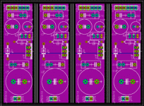
Here is what I have come up with as a final product. I did a big polygon fill to make a ground plane and increased the width of the traces. To me, this board is done unless you guys have any other suggestions.
Chris
An externally hosted image should be here but it was not working when we last tested it.
Chris
Hi triden
I dont know if I understand your design of ground plane. To me it looks like your ground plane dont have any clearance under the solder lugs to those components that not should be soldered to the ground plan. You should have a minimum of clearance of 10-15 MIL out side those drilled holes for a component leg (if using a thru hole component), or else there could be a short. I dont know if you are aware of it but to most PCB design soft wares there is a function/option to choose/specify clearance (in MILs) in the ground plane with respect to the solder lugs.
I agree with Al that your traces are thin, make them thicker or else you could have a risk of getting the linear regulators to oscillate. Also there will be less copper to etch (if doing it by your self) making the etching solution to be active for a much longer period.
You could even have your positive and negative traces (and output traces) as big as small local planes. This will ensure good electrical connections to your filter caps (lower the boards resistance) and improve the circuits performance (e.g. better filtering).
Regards
Re: Hi triden
There is clearance, you just can't see it in the picture. Eagle uses 8mil as the clearance distance between same and different signal traces, pads, and vias. That's fine if your board will have a solder mask layer, but you'll want more if it won't have solder mask. You can change those values by going to Edit>Design Rules>Clearance and playing around with the values. You can also change the thermal clearance values by clicking the Supply tab in the Design Rules window. You can also get rid of the thermals by setting the thermal isolate value to zero.
Like the others said, make power traces as large as possible. Even use a polygon fills if there are lots of connections - like in your circuit.
Check out my regulator circuit for example. The entire bottom layer is a ground plane (polygon fill). Half of the top layer is an input voltage polygon fill. The other half is an output polygon fill. A good PCB design also optimizes paths for high currents to flow. For instance the currents flowing from the input to the regulator, the regulator to the output, and the output ground back to the input ground. These paths should use thick traces (or polygon fills like I used) for low impedance and high current capability. Avoid 90 degree bends when routing traces - only use 45 degree bends. Keep traces as straight and short as possible. I also try to avoid using vias, but other design priorities often make it necessary to use them. There's lots more to PCB design but those are some good basic guidelines.
Flodstroem said:I dont know if I understand your design of ground plane. To me it looks like your ground plane dont have any clearance under the solder lugs to those components that not should be soldered to the ground plan.
There is clearance, you just can't see it in the picture. Eagle uses 8mil as the clearance distance between same and different signal traces, pads, and vias. That's fine if your board will have a solder mask layer, but you'll want more if it won't have solder mask. You can change those values by going to Edit>Design Rules>Clearance and playing around with the values. You can also change the thermal clearance values by clicking the Supply tab in the Design Rules window. You can also get rid of the thermals by setting the thermal isolate value to zero.
Like the others said, make power traces as large as possible. Even use a polygon fills if there are lots of connections - like in your circuit.
Check out my regulator circuit for example. The entire bottom layer is a ground plane (polygon fill). Half of the top layer is an input voltage polygon fill. The other half is an output polygon fill. A good PCB design also optimizes paths for high currents to flow. For instance the currents flowing from the input to the regulator, the regulator to the output, and the output ground back to the input ground. These paths should use thick traces (or polygon fills like I used) for low impedance and high current capability. Avoid 90 degree bends when routing traces - only use 45 degree bends. Keep traces as straight and short as possible. I also try to avoid using vias, but other design priorities often make it necessary to use them. There's lots more to PCB design but those are some good basic guidelines.
Attachments
triden said:Here is what I have come up with as a final product. I did a big polygon fill to make a ground plane and increased the width of the traces. To me, this board is done unless you guys have any other suggestions.
An externally hosted image should be here but it was not working when we last tested it.
Chris
Trimpot pads look awfully small unless you use plated-trough-holes. If you do your own boards you could beef up resistor/capacitor pads also, eagles default size is bit small. Smaller change to tear of a pad if you need to desolder and drilling is easier when there is more copper around hole.
Also, like said already polygon clearance needs a tought, for diy-boards something like 20-40mils work nice.
BTW. You can change Eagle to use mm for units instead of MIL's
from -->View-->Grid
Triden, I really like your board, nice work, you are getting there.
I would make the traces at least twice as wide, I know you are probably thinking that they are fine but no reason not to make them much thicker; esp the main voltage traces as Vin goes through to Vout.
Its hard to see the clearance between the non grounded pins and ground plane, such a close tolerance would make me nervous!
On C2 and R7 there are 2 traces very close together.
On C3 and C5 a trace comes very close to the grounded pin.
On C7, the traces on the neg terminal are dangerously close.
Why is the hole for IC3 way bigger than the other two?
I see you use right angles for some trace turns and angles for others, may want to adjust some of these to have more clearance. As I said if your enter "grid finest" at the command line you will have a finer grid to move the traces around.
The 4 mounting holes look too small to accept a screw. Are you sure that a 4-40 or M3 will fit in there? They look smaller than the leads for the big caps.
Alright guys, I really appreciate your help. Now what I have done is made all the clearances bigger (trace to trace is now 15mill and trace width is 30mil from 20mil), and increased the size of the screw holes. The trimpot holes are correct for the kind of pot going into the circuit. Those faint black lines in the ground plane are traces that run through it. I had to make a couple bottom traces to minimize the distance that they would have had to go if they were on the top. The hole size for the top IC isnt any bigger than the rest, just the restrict area looks to be bigger - not sure why the library had it configured this way. I made the picture a little bit bigger this time so you could see it better
An externally hosted image should be here but it was not working when we last tested it.
- Status
- This old topic is closed. If you want to reopen this topic, contact a moderator using the "Report Post" button.
- Home
- Design & Build
- Parts
- I am really bad at making PCB's