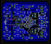
I was attempting to make a few circuit boards in Eagle the other day and after spending hours and hours trying to make the components fit while keeping signals in order I gave up. I did eventually make a "complete" layout for the circuit I was working on (See pics below) but I am not sure it is a good way to go. It is just a simple circuit for a Randy Slone headphone amp and I just wanted to practice laying out components using it. But I just am not happy with it at all. It seems like it got put together only through luck, and not skill at all! ")
So my question is: Are there any general guidelines you pros could give a newbie like me in laying out a circuit, especially when it has multiple pin devices in it such as ICs or chip amp transistors like the LM3886? I mean, with what components should I start? What are some things to keep in mind as far as certain signals being next to certain components? Etc. From what I gather all this comes with experience, but I would like to speed that up a bit, since experience could take a while (I never was all that patient ).
Any tips would help a great deal, I just don't have a very creative brain as far as improvising things like layouts, so any kind of structure to this process will help me and any other like minded DIYer out there.
Thanks!
- Ron
So my question is: Are there any general guidelines you pros could give a newbie like me in laying out a circuit, especially when it has multiple pin devices in it such as ICs or chip amp transistors like the LM3886? I mean, with what components should I start? What are some things to keep in mind as far as certain signals being next to certain components? Etc. From what I gather all this comes with experience, but I would like to speed that up a bit, since experience could take a while (I never was all that patient
).Any tips would help a great deal, I just don't have a very creative brain as far as improvising things like layouts, so any kind of structure to this process will help me and any other like minded DIYer out there.
Thanks!
- Ron
An externally hosted image should be here but it was not working when we last tested it.
An externally hosted image should be here but it was not working when we last tested it.
Searching this forum didn't yield very many direct responses to this sort of question, but going into each project and reading the tips on those specific circuits does help. Thanks for the advice. I just wish there was a more centralized place to learn.
I should note that I have already read the PCB design guide here and am actually asking in this forum for any little tips or advice you all could give for audio specific circuits, as I said especially when IC's/multiple pin chips are involved.
Ron
I should note that I have already read the PCB design guide here and am actually asking in this forum for any little tips or advice you all could give for audio specific circuits, as I said especially when IC's/multiple pin chips are involved.
Ron
Looks fine dude ... and it ain't easy... takes lot of practice to do it fast.
If Eagle lets you do 45's, replace all those 90 deg turns with 2 45's.
If you want it smaller... that just takes work and patience.
As far as the "black magic" is concerned. just keep your outputs away from your inputs... audio is pretty forgiving as far PCB's go.
If Eagle lets you do 45's, replace all those 90 deg turns with 2 45's.
If you want it smaller... that just takes work and patience.
As far as the "black magic" is concerned. just keep your outputs away from your inputs... audio is pretty forgiving as far PCB's go.
Yes, it is a single side, however there is one component on the top side (the 1206 SMT capacitor) but that will actually be going on the bottom side, I just couldn't figure out how to make eagle put it down there so I just left it as is, figuring if I ever made the board I can make it go on the bottom, real close to the two pins it is connected to.
Anyway, what you say about audio circuits is exactly what I thought too (I figured at these low frequencies there shouldn't be anything to worry about) but I think some may disagree on this forum about the audio being pretty forgiving. In fact, this is what most of my confusion rises from. When I go to look at other's projects on this forum and they ask for advice on their PCB layout, usually they get a TON of responses telling them to keep signal A away from those caps, or make sure those traces are short or whatnot. So seeing all of that frustrates me, since I know there are so many suggestions out there and it isn't possible to remember them all.
In any case, I guess a good question I could ask is, how long does it take one of you more experienced DIYers to layout a simple circuit such as the one I have done? This one took me 14 hours and I just never could get into any sort of rhyme or rythm with it.
It depends where you compare it.ron.eddy said:
Anyway, what you say about audio circuits is exactly what I thought too (I figured at these low frequencies there shouldn't be anything to worry about) but I think some may disagree on this forum about the audio being pretty forgiving.
Try fitting SMPS and a mic preamp on same board if you like challenges
Where you are going to connect those bypass cap gounds together? AD797 is usually tought as tricky nut to bypass compared to any other audio-opamp. Aim to keep total trace+component lenght minimal between supply pins, bypass caps and ground.
I usually start with bypass cap placement, then feedback resistors and after that rest of the stuff where it fits. Dont be shamed to use jump wires on 1-side board, its way more better to use couple of jumps than run signals around the board in loops trying to not use jumper wires. Some people seem to rate pcb layout by amount of jumpers used, thinking that less is better.
Mike Gergen said:Practice, practice, practice.
Yea, good plan. It is fun, in an odd sort of way.
mzzj said:
It depends where you compare it.
Try fitting SMPS and a mic preamp on same board if you like challenges
Yea, by no means am I saying that there is no need for care with PCB layout, just wondering was all.
Where you are going to connect those bypass cap gounds together?
I was going to connect them to the main chassis ground via jumper wires. I was under the impression that the ground lead length is not as important as the signal lead length, which I have kept under 5mm as per AD797 datasheet recomendations, so should I also be worrying about the ground trace length as well?
I usually start with bypass cap placement, then feedback resistors and after that rest of the stuff where it fits. Dont be shamed to use jump wires on 1-side board, its way more better to use couple of jumps than run signals around the board in loops trying to not use jumper wires. Some people seem to rate pcb layout by amount of jumpers used, thinking that less is better.
This is the exact kind of advice I am looking for. Personal experiences and what you all like to do first, second, whatever. Thanks for the input.
- Ron
Some general concerns are: Ground as much as possible in a star fashion to 1 point. Different current paths to ground rather than sharing the same path, especially the higher current paths. 1 giant ground plane is ussually acceptable as 1 point. Keep signal paths short like you suggested, especially low level and or high impeadance paths(OpAmp inputs). If any radiaded noise will be picked up the longer traces act somewhat like more turns on a transformer and the noise voltage will be higher. Lower impeadance areas of the circuit are less sensitive to noise pickup(Outputs) keep this in mind when you have to make a decision between the two. I ussually get the Rs associated with a high Z area very close to the pin. This leaves the ussually lower impeadance side of the resistor with the longer trace. And diffinatly keep inputs away from outputs as much as possible. I'm little surprised these SMPS guy's don't step right up and teach us all. They are some of the most difficult circuits to layout cleanly. They have all the difficult parameters to deal with on the same circuit. As for the guy with the mic pre on the same board with a switcher, He should be proud, I wouldn't even bother trying!
Thank you for that advice, I used it, along with the other advice to make a new layout for the circuit. I was able to reduce its size by 50% in the mean time. This is odd because I have been looking at this circuit for days and not knowing how to improve it and now with just a couple pointers it is already making much more sense.
SMPS circuits have high frequency to worry about, making it pretty difficult, is that correct? (Excuse for my unfamiliarity with these circuits)
SMPS circuits have high frequency to worry about, making it pretty difficult, is that correct? (Excuse for my unfamiliarity with these circuits)
An externally hosted image should be here but it was not working when we last tested it.
Another question I have involves the ground plane. My grounds in this circuit are kept separate, so as to facilitate their connection to a high quality ground point. With that said, is there any benefit to still using a copper fill on the board and attaching it to the metal chassis (which of course will be grounded)?
I plan on doing it anyway because it will be easier to etch then, but is there any benefits from it? In the picture below you will see the copper pour is not connected to any of the "HQG" connections.
Thanks, Ron
I plan on doing it anyway because it will be easier to etch then, but is there any benefits from it? In the picture below you will see the copper pour is not connected to any of the "HQG" connections.
An externally hosted image should be here but it was not working when we last tested it.
Thanks, Ron
If you use a copper pour, make sure there are no isolated "islands" left on your board, and the copper should always be connected to earth. Power ground is fine, but if you really want to get fussy, you can run it separately back to chasssi star ground.
Star ground all signal earths, and if you have enough copper left, then you can use a ground plane for power grounds.
Swap C9 and C7 around so the smaller cap is nearest the IC pin. that will help with stability.
If this was one of my designs I would have done things slightly differently. I would have started my design at 90 degrees to yours, and run two power rails right up the middle of the board then I would have built the circuit as symetrically as possible, stating with PSU decoupling then moving out, as Mzzj suggests.
Here's a design I'm working on at the moment that shows some of these aspects:
Attachments
ron.eddy said:
I was going to connect them to the main chassis ground via jumper wires. I was under the impression that the ground lead length is not as important as the signal lead length, which I have kept under 5mm as per AD797 datasheet recomendations, so should I also be worrying about the ground trace length as well?
Page 13. fiq. 35. 5mm for ground trace lengt. Try wide ground track under chip and bypass caps over and under chip.
pinkmouse said:
If this was one of my designs I would have done things slightly differently. I would have started my design at 90 degrees to yours, and run two power rails right up the middle of the board then I would have built the circuit as symetrically as possible, stating with PSU decoupling then moving out, as Mzzj suggests.
Actually, that is exactly how I started out doing it, but for some reason I was running into a lot of trouble with the transistors. So I separated the +15 and -15 to different sides of the board and then laid out semi-symmetrically from there, starting with PSU decoupling. I changed around those caps as you said and they actually fit a lot better this way.
Below is what I have so far (Without the pour), and as you can see the +15 side is above the AD797 and the -15 side is on the bottom. The input is in the center very close to the input pin of the op-amp (I don't know if this is a good idea or what, maybe someone has some input on that???), the output is on the left side in the middle (vertically):
An externally hosted image should be here but it was not working when we last tested it.
mzzj said:
Page 13. fiq. 35. 5mm for ground trace lengt. Try wide ground track under chip and bypass caps over and under chip.
Ah, I see. I read that wrong the first time I looked at it. But I was wondering, out of curiosity, why the length of that ground track would be so critical, as it still has a ways to go before the signal going into the ground trace actually gets to earth. I mean, realistically, it is going to be seeing the small trace, the wire to attach that ground to the chassis, then the wire from the chassis to the outlet, then the wire from the outlet to earth. Does the ground trace on the bypass caps have to be that critical given these circumstances? I guess I do not understand fully.
I think I got the caps close enough now to the power pins, but since the lead separation on the bigger of those two caps is 5.08mm, there is no way to get the total path (caps and all) under 5mm, no matter what I do.
On a more general note, when any of you start laying tracks for a circuit board do you break the circuit into functional blocks (i.e. input section) and then base the circuit around those, or do you go more by the schematic and electrical connections? (i.e. as long as they are connected it matters little where on the board they are located (with some exceptions of course))
- Thanks a bunch,
Ron
Hi Ron
I may be a little confused, but I still don't see a star for signal grounds.
The important thing with the supply bypassing for the IC is to get the small caps as near to the power pins as possible, the position of the bigger ones isn't quite so critical.
It may seem silly, but to me, the problem with your board is symmetry, or lack of it. It just looks wrong. The basic circuit is the same for each side, left and right, so why is your board so different from the left to the right channel?
I use a combination of laying out functional blocks aand following schematics, (sort of!). If you look at my board, you can see the complete blocks for the CCSs on the right, as they are fairly self contained modules, as is the relay driver section on the left. The other bits are just initially roughly laid out to follow the schema, but then moved and adjusted to suit track lengths, clearances, and other design criteria...
I may be a little confused, but I still don't see a star for signal grounds.
The important thing with the supply bypassing for the IC is to get the small caps as near to the power pins as possible, the position of the bigger ones isn't quite so critical.
It may seem silly, but to me, the problem with your board is symmetry, or lack of it. It just looks wrong. The basic circuit is the same for each side, left and right, so why is your board so different from the left to the right channel?
I use a combination of laying out functional blocks aand following schematics, (sort of!
). If you look at my board, you can see the complete blocks for the CCSs on the right, as they are fairly self contained modules, as is the relay driver section on the left. The other bits are just initially roughly laid out to follow the schema, but then moved and adjusted to suit track lengths, clearances, and other design criteria...The star ground is not on the board, it is actually going to be right next to the mounting position of the board attached to the chassis. I only did this because my grounds were all broken up on the board and were gonnna all need jumper wires to get to ground anyway, so I will just jumper them all to a high quality ground individually.
I see what your saying about the symmetry. I will probably attempt another go at this board tonight or tomorrow to see if I can make one more symmetrical. This is a single channel of the amplifier, so with single sided and given the schematic I could not find a way to make it symmetrical other than a few items (The output transistors, the +/15v inputs, etc). But I will try your suggestion of power and ground up the middle.
Thanks for the advice,
Ron
- Status
- This old topic is closed. If you want to reopen this topic, contact a moderator using the "Report Post" button.
- Home
- Design & Build
- Parts
- Amplifier PCB Layout Guidelines?