Hey, All!
I'm a noob to designing audio PCB layouts, and would enjoy hearing some feedback on this bridging adaptor.
The circuit is from Rod Elliot's web site: http://sound.westhost.com/project14.htm
I intend for this board to eventually go in front of an LM3886 chip-amp on the odd occasion when I need loud mono sound (stage monitor duty). So noise and such isn't a huge concern (everything else in the chain is already noisy.. argh), but I'd like to eliminate as much as possible at the design stage.
It will be built on 2lbs copper SS fibreglass board with no through-hole plating.
Design "principles":
I tend to use thick traces and pads because I have a hard time etching the small stuff accurately (0.02" is about my limit) and the trace edges sometimes come out a little porous. I tend to leave a big gap between the edge of the board and the circuit because cutting fibreglass with a dremel tool is not the easiest thing to do accurately. I guess I need to buy a better laserprinter and a bandsaw... Anyhow.")
Additional principles not rooted in manufacturing technology: I've noticed that most audio and RF boards I've seen leave a huge ground plane, run signals parallel to grounds, don't do sharp bends, and keep the signal paths as short as possible. I honestly don't fully understand why all of that is (they never really covered AC in highschool electronics, YEESH), so for the better part, I'm just mimicking other designers.
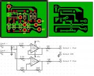
Input is at the bottom, output is on the right. TL072 op-amp, half running NI the other half running inverted. Input will be from a panel-mounted RCA jack, output will probably also be RCA jacks, with external patch cables to the chip amp inputs -- I don't want to run my chip amp inputs through a switch when I'm not using the bridge.
The Chip amp board and this board will have a common ground, I'm not sure yet where I'm going to get the 15V rails for the TL072 from. The chip amp will have 35V rails.
(Should I add caps from the TL072's supply lines to ground?)
Wes
I'm a noob to designing audio PCB layouts, and would enjoy hearing some feedback on this bridging adaptor.
The circuit is from Rod Elliot's web site: http://sound.westhost.com/project14.htm
I intend for this board to eventually go in front of an LM3886 chip-amp on the odd occasion when I need loud mono sound (stage monitor duty). So noise and such isn't a huge concern (everything else in the chain is already noisy.. argh), but I'd like to eliminate as much as possible at the design stage.
It will be built on 2lbs copper SS fibreglass board with no through-hole plating.
Design "principles":
I tend to use thick traces and pads because I have a hard time etching the small stuff accurately (0.02" is about my limit) and the trace edges sometimes come out a little porous. I tend to leave a big gap between the edge of the board and the circuit because cutting fibreglass with a dremel tool is not the easiest thing to do accurately. I guess I need to buy a better laserprinter and a bandsaw... Anyhow.
Additional principles not rooted in manufacturing technology: I've noticed that most audio and RF boards I've seen leave a huge ground plane, run signals parallel to grounds, don't do sharp bends, and keep the signal paths as short as possible. I honestly don't fully understand why all of that is (they never really covered AC in highschool electronics, YEESH), so for the better part, I'm just mimicking other designers.
Input is at the bottom, output is on the right. TL072 op-amp, half running NI the other half running inverted. Input will be from a panel-mounted RCA jack, output will probably also be RCA jacks, with external patch cables to the chip amp inputs -- I don't want to run my chip amp inputs through a switch when I'm not using the bridge.
The Chip amp board and this board will have a common ground, I'm not sure yet where I'm going to get the 15V rails for the TL072 from. The chip amp will have 35V rails.
(Should I add caps from the TL072's supply lines to ground?)
Wes
Attachments
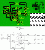
1st basic rule for designing layouts : do not run signal traces parallel to one going from or to high value resistors, or if needed place a ground trace inbetween.
2d rule: keep input and output far separated from eachother.
The trace from R6 going to output W3 is in parallel with the one supplying R1, R2 and R3 from input W2.
I'd lay a ground trace inbetween those two.
The trace connecting R2 and R5 is in parallel with the one connecting R4 and Pin 5. R2 and R5 are 100K.
You're a good copycat.
for +- 15v regulated, an easy way out is to take a PTB48510CAH from TI, remove the pins, and put in wires. Or, make your pcb to accept the module. They will give you one as a sample.
Also, a super easy bridging adapter is made by using the DRV134 from TI. they'll also give you up to 5 of those as a sample.
Also, a super easy bridging adapter is made by using the DRV134 from TI. they'll also give you up to 5 of those as a sample.
Hey, Guys!
Thanks for the useful feedback!
> You're a good copycat.
I'll take that as a compliment.
I tried re-working my original board, but wound up doing another one from scratch. Thank God for schematic-netlist-PCB integration!
I found keeping those signals apart from each other is very tricky, given the layout of the op-amp! Is there any problem with running signals underneath resistors as I've shown? I use this "trick" often in other applications (usually to avoid making a 2-sided PCB or running jumper wires).
Also, is there any benefit to using a two-sided board, and just making one whole side ground? (Since I can't etch two-sided accurately anyhow).
BigMike: PTB48510CAH -- Gah! Have you priced those?? $79 from Digikey, minimum order of 9. The sample route is a good idea, but I prefer to own equipment I can afford to repair! (What can I say, I'm a clumsy guy... Broke a PCB yesterday stressing the leads of a TO-220 device via it's heatsink on the chassis. GRR!)
DRV143 -- Excellent idea. Got any schematics around? I'm going to read the datasheet more carefully and see what I can come up with.
Attached is my revised PCB. Should this be relatively noise-free? (Noise in this context only counts where it could be eliminated by PCB design.
Also, is there a noise benefit to adding a capacitor from the + to the - rail near the chip? Or from each rail to ground? I know SRAM chips and such always have a ~0.1uF "debouncing" cap installed right at the chip, but I'm not sure if this is a benefit to audio applications. I don't see it near op-amps very often in stuff I've opened.
Cheers,
Wes
Attachments
The 0.1uF caps -- normally rail-to-rail or rail-to-ground?
Do you know how that oscillation works? Is it because when the load switches on, that causes a slight drop or spike in the reference voltage, causing it to switch off again, and start the cycle anew? Or is there something "trickier" going on there?
Thanks,
Wes
Do you know how that oscillation works? Is it because when the load switches on, that causes a slight drop or spike in the reference voltage, causing it to switch off again, and start the cycle anew? Or is there something "trickier" going on there?
Thanks,
Wes
- Status
- This old topic is closed. If you want to reopen this topic, contact a moderator using the "Report Post" button.
- Home
- Design & Build
- Parts
- First Audio PCB Designed -- Comments?