Hi all,
I've got some problems fixing this
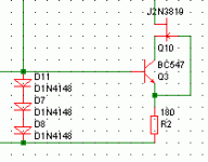
The schematic is included, Q3 Q10 and the diodes form a CCS (I hope so)
Q10 seems to cascode the BJT.
Without Q10 the CCS works correctly, but when Q10 is here, the BJT draws 1mA (!!!) on its base, and Vref (on the diodes) becomes bad.
Is something wrong on the schematic?
Thanks for help
I've got some problems fixing this
The schematic is included, Q3 Q10 and the diodes form a CCS (I hope so)
Q10 seems to cascode the BJT.
Without Q10 the CCS works correctly, but when Q10 is here, the BJT draws 1mA (!!!) on its base, and Vref (on the diodes) becomes bad.
Is something wrong on the schematic?
Thanks for help
I think I can see the problem. The current is set at about 7mA, and if you look at the datasheet for the 2N3819, its Vgs is only a fraction of a volt at that current. It's impossible for the BJT to operate with that little potential difference between emitter and collector, so the circuit cannot function as expected.
So, you either need to find a different FET, or reduce the current it is to pass.
So, you either need to find a different FET, or reduce the current it is to pass.
Can someone tell me what Jfet would work for this application?
The 2N3819 and U404 (the models simetrix knows) don't simulate well. I found models on the internet for the BF245 (model from philips), U308/309/310 (from fairchild), the BF245C is ok (A and B versions aren't), the U308/309 don't give much headroom to the BJT, and the U310 seems ok.
But in real life, which one should I choose? Current is approx 6mA.
BF245A: Vce=0.040V
BF245B: Vce=0.060V
BF245C: Vce=1.600V
2N3189: Vce=0.050V
U308: Vce=1.610V
U309: Vce=0.870V
U310: Vce=1.98V
U401: Vce=0.050V
1.6V will generally be ok for a small-signal BJT, however it depends on the particular device. In the datasheet, look at the graph(s) of Vce against Ic. It will show that as Vce decreases, IC remains fairly constant until at a certain point it starts to drop to zero. Don't go below that point and the BJT will be happy.
As for the JFET: since I never use them due to hardly any being available, my knowledge of them is limited, but it seems to me that for this application, higher Idss and lower (more negative) Vto will avoid the problem you had. The graph of Vgs against Id in the datasheet can tell you how it will behave at the required current.
As for the JFET: since I never use them due to hardly any being available, my knowledge of them is limited, but it seems to me that for this application, higher Idss and lower (more negative) Vto will avoid the problem you had. The graph of Vgs against Id in the datasheet can tell you how it will behave at the required current.
Bricolo said:Vcesat for the BC550 is 0.6V max (that's small!
I'll try with a J310, as I have some of them laying around.
Can someone confirm that J310 and U310 are similar?
Datasheet at www.vishay.com ?
Google perhaps?
Angry?
Salut Bricolo,
Me angry?, absolutely not. Come on!
Bricolo said:I didn't check vishay's datasheet but onsemi's ones, and the values and cuerves are very close
Don't become angry Elso
Salut Bricolo,
Me angry?, absolutely not. Come on!
It's not my work, but I can't explain this choice
I juste tried to use the schematic I had, but hadn't the same jfet. And my J309 (from onsemi) didn't work well
I'll try this week if I have some time (and if I can borrow a power supply at the university) with a J310 that simulates ok.
If some of you have a spare power supply to sell, I'm interested. Something with dual voltage output; to make +-
- Status
- This old topic is closed. If you want to reopen this topic, contact a moderator using the "Report Post" button.
- Home
- Design & Build
- Parts
- BJT cascoded with a Jfet: how can I make it work?