You need to be a bit more thorough with your searches:
http://www.diyaudio.com/forums/solid-state/123613-class-biasing-ad797-2.html#post1525757
Is the closest I remember. "jcx" and "ad797" gets you pretty far though.
http://www.diyaudio.com/forums/solid-state/123613-class-biasing-ad797-2.html#post1525757
Is the closest I remember. "jcx" and "ad797" gets you pretty far though.
yes, I do need to be more thorough, but I do need help please.
That link did not help me.
Just to be sure, you saw the .asc at the bottom? Scott's own comments were that JCX got pretty close. There's the AES preprint describing the circuit design, but I haven't read it.
There's still relevant reasons AD wouldn't want to have every last bean spilled about it, even ~30 years later, as it's still one of their highest performing precision, low noise opamps.
This was published at the AES, the bias currents are all ordinary current sources and the Ib comp and null are not shown but they are nothing special. I have retired and all my archives are no longer with me. If you have a question I can probably answer it here.
Attachments
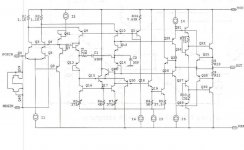
Intriguing with the circuit around Q23 and associated bits. Is that a saturation clamp of sorts?
Tom
Q23 is just a cascode for Q19. There are clamps in the current mirror shown for both + and - misbehavior (Q50, Q64).
EDIT - Obviously C2 does not go to chassis ground, I honestly don't remember how the metal layers and parasitics were actually wired.
Last edited:
I believe that Q18 and Q19 are a bootstrap to keep the VCe of Q17 constant, regardless of signal level.
They bootstrap all the pairs of devices in the stage, in an ordinary circuit they would be the Vas devices and the voltage gain would be at best a few 100's of thousand's. This way what would be the Vas error voltage becomes a common mode error and a single gain stage achieves >5-10Meg. The input still sees the current burden of the output buffer as a differential error so it had to be a triple darlington with cascode from the output voltage.
Last edited:
i had this crazy idea of cascading two chips for more gain but i do not need the current gain of both chips. so i was looking at where i might access just the voltage gain stage.
thanks
The other side of the gain stage, (at R3, the opposite sense of where C2 is connected) is pin 8 on the IC. This would be the output unbuffered. I have heard folks put a resistor to ground here and use the part open-loop. Stuff like this needs some care and I have not tried any of it. If you can I would use John's (jcx) LTSPICE files and play around. For this the schematic here gives you all the info you need, some decent discrete models with around 600 MHz ft should be OK.
Your best bet in general would be to research the various composite amplifier schemes, there are lots of ways to skin that cat.
another discussion about AD797
Headphone Amp - AD797 compensation, distortion cancellation caps
Headphone Amp - AD797 compensation, distortion cancellation caps
- Status
- This old topic is closed. If you want to reopen this topic, contact a moderator using the "Report Post" button.
- Home
- Design & Build
- Parts
- AD797 schematic