First I have to say that I'm not a native electronician. I studied mechanics first and learn way after electronics by reading old HiFi tubes books and more modern hifi magazines that were having a nostalgic look to famous tube amp schematics like Marantz 9B, Audioresearch D series, McIntosh, Dynaco and a few others I forgot.
So all my apologies if my tech vocabulary is not up right, besides that english is not my native langage.
After having dreamed on the magics of tubes, I played a while with some williamson's and Loyer's designs and finally decided to go with "my own" design.
I went up with a PP of 6550C cathode loaded, driven by a Mu follower composed with a 6SN7 topped with a 6au6 penthode. There's two stages before, the phase splitter with unity gain, and a differential stage used to improve signal symetry and balance AC output. There's only some local feedback due to the cathodes loads and no overall FB loop. The amp develop 30W output power, being in class A up to 25W. Bandwidth as far as I remember from a few herz to 20kHz at less than one db. Distorsion is kept very low for an open loop.
It's still running as a single channel prototype. Beside some obvious qualities as details and dynamics, I still have some work to improve bass rendering and work on bias stability.
Didn't want bypassed cathode resistor for the bias and the minmum amount of caps out of the PS, so there's a direct connection between the driver and the power tubes.
The driver is supplied between +300v/-540v so the output driver voltage may drift by 2 or 3 volts depending of the series regulated power supply or tubes temperature.
The plan is to first adapt a pair of Salas HV shunt PSU on the driver and also adapt a Broskies type Auto-Bias. The bias regulation will read the bias current on two low R resitors between primary windings and ground and symetrically act on 6AU6 screen voltage and 6SN7 cathode voltage to keep the same idle current on the Mu follower whatever the bias voltage.
That's where I'm in trouble, I'm having a hard time to find comlementary BJT able to regulate with a few mAmps (2 to 5) with up to almost 600V across them. Most of the HV trans easily available on the market (mje15034/mje15035 ; MJE340-350 ; KSC3503/KSA1381) have a VCE that hardly goes over 300V. So the only way to use them would be to share the voltage across two units.
There's switching devices that go higher in voltage and current but I'm not sure they would fit to the purpose. Are we going into a penury of High voltages linear transistors ? Power mosfet may be a solution but for a few mAmps ?
Do you have sources to get such devices except from your personal drawers ?
Thanks for your help.
with CRT going the way of the dodo lots of hi V bjt are following
V regulators in general, tube circuit regulators in particular are most often single ended
there are a few MOSFET of reasonably small size for hi V - some N-channel are even depletion mode and can look a lot like a tube
V regulators in general, tube circuit regulators in particular are most often single ended
there are a few MOSFET of reasonably small size for hi V - some N-channel are even depletion mode and can look a lot like a tube
2SC3675 10W, Collector-Emitter Volt (Vceo): 900V, Collector-Base Volt (Vcbo): 1500V. I used them for focus modulation in CRT video projectors (100 khz horizontal sweep) still available.
https://www.futurlec.com/Transistors/2SC3675pr.shtml
https://www.futurlec.com/Transistors/2SC3675pr.shtml
Last edited:
I have never seen a linear BJT, at any voltage. They are not supposed to be linear!Laurent33 said:Are we going into a penury of High voltages linear transistors ?
Find a BJT which can cope with the voltage, and try it.
I have never seen a linear BJT, at any voltage. They are not supposed to be linear!
Find a BJT which can cope with the voltage, and try it.
I believe that Laurent seeks a HV bipolar which is optimised for (and specified for) linear applications, rather than one specified for switching applications.
The linear-application types have data sheets giving more information on capacitance behaviour, Hfe variation in the linear region, Hfe flatness with collector current, saturation behaviour. There are fewer of these now, as jcx says, due to the loss of the CRT applications. Switching types have optimisation for switching-time and low Vce at saturation. Hfe variation with collector current matters little here, and often it is far worse than older linear-optimised types.
OK. I wondered if that is what he meant, but as a self-confessed newbie I thought he may be under the impression that he needs a linear BJT to get linear amplification.Rod Coleman said:I believe that Laurent seeks a HV bipolar which is optimised for (and specified for) linear applications, rather than one specified for switching applications.
Thanks to all for the HV references I missed. I'll try some and fill my drawers in case of complete extinction.
I was looking first for a complementary pair of HV devices to act on both ends of the driver but I didn't know that HV trans in P flavor are rare as BJT (but all are switching devices and SMD package) and simply doesn't exist as MOSFETs.
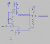
Anyway, I better switch to a single ended design with a NPN across the 840v of the driver's Voltage supply. Thanks for the zener stack idea, it will allow me to drive it with a NPN with lower voltage capability. Something like that :
As for the term "Linear", I referred to some datasheets that oppose linear applications to switching. I did not know much what it implied but thought it would not be good to use high power switching devices for small current DC regulation.
I was looking first for a complementary pair of HV devices to act on both ends of the driver but I didn't know that HV trans in P flavor are rare as BJT (but all are switching devices and SMD package) and simply doesn't exist as MOSFETs.
Anyway, I better switch to a single ended design with a NPN across the 840v of the driver's Voltage supply. Thanks for the zener stack idea, it will allow me to drive it with a NPN with lower voltage capability. Something like that :
As for the term "Linear", I referred to some datasheets that oppose linear applications to switching. I did not know much what it implied but thought it would not be good to use high power switching devices for small current DC regulation.
Attachments
Give us a schematic (even simplified) of what exactly you have in mind and we will find a way to do without Bjt'sThe bias regulation will read the bias current on two low R resitors between primary windings and ground and symetrically act on 6AU6 screen voltage and 6SN7 cathode voltage to keep the same idle current on the Mu follower whatever the bias voltage.
Give us a schematic (even simplified) of what exactly you have in mind and we will find a way to do without Bjt's
One post up.
One post up.
Ok, here are two ideas, based on opto's: first is opto-extremist, 100% opto, second is hybrid and uses one opto and one MOS.
Topology and values have been dimensioned to ~suit your apparent requirements (I don't have all the info). You can easily correct the gain, offsets, etc yourself.
Note that even if some BJT's are available with a Vce in excess of 1.8kV, the SOAR shrinks to zero beyond ~500V, making them useless for linear applications.
MOS are better in this respect, and you can easily find a 1kV NMOS perfectly usable in linear regime
Attachments
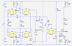
Ok, here are two ideas, based on opto's: first is opto-extremist, 100% opto, second is hybrid and uses one opto and one MOS.
Thanks, that's an elegant and efficient solution while the "hybrid" one makes more sense to me.
One question please : While the base of the opto's output transistor is driven internally by the led, why is the base available and not connected on the output ? Is it a possibility to establish a quiescent current in case of AC connection on the input ?
Note that even if some BJT's are available with a Vce in excess of 1.8kV, the SOAR shrinks to zero beyond ~500V, making them useless for linear applications.
I expect to draw between 1 to 3 mA on the HV trans. There's almost always some room for such a small current next to the max voltage on the trans I had a look to. I can also stick a resistor on the collector to decrease VCE as you did on your hybrid solution.
The choice between BJT and mosfet would be about reliability. I have no idea on parameters or safe design to look at for such a choice, beside I always heard MOS as being "sensitive devices". Same for optos a few years ago, while it looks like they can be very reliable devices now.
I do not see clearly what you exactly mean: the photo current is generated in the B-C space, and contributes to the base current, but also to the collector and emitter currents, since you see the device as a dipole when it's open base.Thanks, that's an elegant and efficient solution while the "hybrid" one makes more sense to me.
One question please : While the base of the opto's output transistor is driven internally by the led, why is the base available and not connected on the output ? Is it a possibility to establish a quiescent current in case of AC connection on the input ?
If you connected the base to the output, you would change your transistor into a diode, having a Vbe only marginally influenced by the light.
The base is accessible for other purposes: for example, in the first part of my schematic, I have included 15V zener diodes to clamp the maximum voltage in case something goes wrong (15V supply lost for example).
With a bit of ingenuity, you could replace the zeners by dividers going to the bases, but I didn't do it, because you have to be careful not to shunt the photocurrent during normal operation, and this could be quite delicate: I opted for the simple and safe solution, but anyway, the cost to be gained by replacing a single zener by two resistors and probably a diode seems minimal and not worth the trouble
Yes, if you search, you can find bipolars having a little bit of spare area on the right: the BUY89, a 800V/1.5kV transistor still tolerates a hefty 30mA at 800V, but it is an exception.I expect to draw between 1 to 3 mA on the HV trans. There's almost always some room for such a small current next to the max voltage on the trans I had a look to. I can also stick a resistor on the collector to decrease VCE as you did on your hybrid solution.
The choice between BJT and mosfet would be about reliability. I have no idea on parameters or safe design to look at for such a choice, beside I always heard MOS as being "sensitive devices". Same for optos a few years ago, while it looks like they can be very reliable devices now.
MOS are categorized as sensitive, because they are mostly unprotected (the gate), and they could be zapped by poor handling. That is the theory, and I have verified it very occasionally, but the truth is that large MOS have a few nF gate capacitance, and in order to charge that capacitance to a dangerous voltage, you really have to be careless or very unlucky.
The only ones I managed to zap were low power types, BSxyz, having a much smaller gate capacitance.
Other than that, MOS are much more resilient than BJT's for HV linear operation. This doesn't mean you are allowed anything and everything, but they are actually usable provided you follow some basic health guidelines.
I have described a number of MOS-based HV linear circuits, mainly supplies, and in practice they proved rugged enough.
With BJT's, it would be much much trickier.
I do not see clearly what you exactly mean.
Sorry, I was just wondering about base availability purpose on HV side. Not thinking to use it on the current subject.
Thanks Elvee for the help, I'll give MOSFETs a try.MOS are categorized as sensitive, because they are mostly unprotected (the gate), and they could be zapped by poor handling. That is the theory, and I have verified it very occasionally, but the truth is that large MOS have a few nF gate capacitance, and in order to charge that capacitance to a dangerous voltage, you really have to be careless or very unlucky.
The only ones I managed to zap were low power types, BSxyz, having a much smaller gate capacitance.
Other than that, MOS are much more resilient than BJT's for HV linear operation. This doesn't mean you are allowed anything and everything, but they are actually usable provided you follow some basic health guidelines.
I have described a number of MOS-based HV linear circuits, mainly supplies, and in practice they proved rugged enough.
- Status
- This old topic is closed. If you want to reopen this topic, contact a moderator using the "Report Post" button.
- Home
- Design & Build
- Parts
- Hard time to find High Voltage medium power linear BJT