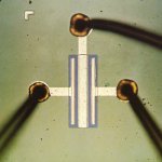
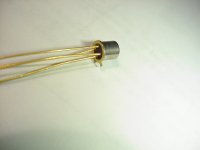
I was at Fairchild Semiconductor in 1966 and picked up these unmarked devices in the engineering department. The die in the pic is in a TO-72, which has 4 leads, one is the case and the other three go to the die. The die is about 0.5 mm. What is the device type and what are connections?
Attachments
A NPN/PNP transistor has a collector , base and emitter , Looking at the transistor the second pin would appear to be the base (or the P or N in a NPN or PNP transistor) the other two are either the collector or emitter .....
Put it in a basic transistor curcuit with a socket and try it both ways and see which one works and you should be able to figure out the pinout from there ....
it is most likely a NPN if it is from the 60"s ......
You might also be a ble to deduce the pinout with the transistor setting on your DMM .....
Cheers
Are you sure that's not a FET with both gates leaded out?
I think you are on to the right track thinking it's a FET. In the '60 we called them MOST....for Metal-Oxide-Silicon-Transistor. MOST never caught on, MOSFET is a better acronym.
This is a dual gate MOSFET die, my device has one gate.
Attachments
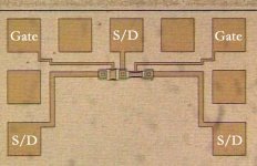
The device is an Enhancement Mode P-Channel MOSFET.
The 3N164 has similar characteristics.
http://www.datasheetcatalog.org/datasheet/linearsystems/3N163-4.pdf
The 3N164 has similar characteristics.
http://www.datasheetcatalog.org/datasheet/linearsystems/3N163-4.pdf
Attachments
In 1959 M. M. (John) Atalla and Dawon Kahng at Bell Labs achieved the first successful insulated-gate field-effect transistor (FET), which had been long anticipated by Lilienfeld, Heil, Shockley and others (1926 Milestone) by overcoming the "surface states" that blocked electric fields from penetrating into the semiconductor material. Investigating thermally grown silicon-dioxide layers, they found these states could be markedly reduced at the interface between the silicon and its oxide in a sandwich comprising layers of metal (M - gate), oxide (O - insulation), and silicon (S – semiconductor) - thus the name MOSFET, popularly known as MOS. As their device was slow and addressed no pressing needs of the telephone system, it was not pursued further. In a 1961 memo, however, Kahng pointed out its potential "ease of fabrication and the possibility of application in integrated circuits." But researchers at Fairchild and RCA did recognize these advantages. In 1960 Karl Zaininger and Charles Meuller fabricated an MOS transistor at RCA and C.T. Sah of Fairchild built an MOS-controlled tetrode. Fred Heiman and Steven Hofstein followed in 1962 with an experimental 16-transistor integrated device at RCA.
The MOS transistor conducting region is either p-type (making it a "p-channel" device) or n-type ("n-channel" device) material. The latter are faster than p-channel but are more difficult to make. MOS devices hit the commercial market in 1964. General Microelectronics (GME 1004) and Fairchild (FI 100) offered p-channel devices for logic and switching applications; RCA introduced an n-channel transistor (3N98) for amplifying signals. Because of their smaller size and lower power consumption than bipolar devices, over 99 percent of microchips produced today use MOS transistors. Achieving such ubiquity took decades of effort.
Computer History Museum - The Silicon Engine | 1960 - Metal Oxide Semiconductor (MOS) Transistor Demonstrated
- Status
- This old topic is closed. If you want to reopen this topic, contact a moderator using the "Report Post" button.
- Home
- Design & Build
- Parts
- DIE IDENTIFICATION