Hi,
I have a few 2SK146 Toshiba dual jfet devices that I am planning to use to build an phono preamp.
However, I just realized that it seems impossible to find the pinout configuration anywhere...
Is anyone aware of that knowledge and able to share it in this site, please?
Thanks!
I have a few 2SK146 Toshiba dual jfet devices that I am planning to use to build an phono preamp.
However, I just realized that it seems impossible to find the pinout configuration anywhere...
Is anyone aware of that knowledge and able to share it in this site, please?
Thanks!
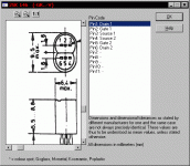
Well, after much digging around, I found this Japanese site, where pin-outs can be checked for 2SK146 dual JFET, and also the 2SK147 single JFET (the 2SK146 contains two 2SK147 in a single aluminum capsule, where one uses Series A pin-out and the other one uses series B pin-out, and in this way, both Drain and Source pins are located side by side):
2SK101-200
However, my Japanese is not good enough (cough, cough...), so I have used, guess what, our friend Google to translate one or another word:
東芝 => Toshiba
2SK147のDualタイプ => Dual type 2SK147
SOURCE => ソース
GATE => ゲート
DRAIN => ドレイン
So, I came out with the following pin-out comfiguration for the 2SK146 dual JFET packages:
The top notch on the capsule will tell us where to find pin 1.
Any one can comment on this?
I hope to do some testing to find out the IDSS and Vp for my 2SK146 GR H2 devices soon..
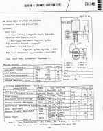

") Thanks for the datasheets, hard to find anywhere else in English!
Thanks for the datasheets, hard to find anywhere else in English!- Status
- This old topic is closed. If you want to reopen this topic, contact a moderator using the "Report Post" button.
- Home
- Design & Build
- Parts
- 2SK146 Dual JFET matched pair pinout