Quick question....
For switching lots of fets (2250pf gate capacitance each and there five of them) should I incorperate a extra strage to my PSU which give a extra 10v on my rail voltage and use a bipolar stage for switching them? (like the ESP SMPS)
also is it possible to saturate the transisters by having a 25v base signal and have it switching ~50v?
any better surgestions would be appreciated")
Thanks all
For switching lots of fets (2250pf gate capacitance each and there five of them) should I incorperate a extra strage to my PSU which give a extra 10v on my rail voltage and use a bipolar stage for switching them? (like the ESP SMPS)
also is it possible to saturate the transisters by having a 25v base signal and have it switching ~50v?
any better surgestions would be appreciated
Thanks all
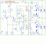
Do you have a diagram? Do you mean like the mosfet driver stages here? BTW the junction FET constant current source here needs to be replaced with another type which can handle higher voltage. V9 and V10 could be mosfets with the gates tied to the drains and sources by means of potentiometers and be mounted on the heatsinks for thermal compensation. I don't know if the circuit works since I was only able to simulate it.
Attachments
Frequency is about 100khz, Current can be almost anything as i'm just adding windings to a 10kw torroid of a SMPS for a car amp.
its for a class D amp whereby a lm4651 give out a 25v pulse (typically use for a integrated H bridge) @ 100khz to the music and the rail being swithed is about 47v.
As far as I figured I'd have a PNP and NPN on thier respected rails (one GNS the other VCC+10v) driven off the same pulse so that when ones on the others off at all times. The outputs would be tied to the array of fets with each fet having its own charge/discharge resistor. FAirly simialar to the schematic posted.
Is it gonna work?
frOst,
There are many interrelated issues here. The switching freq itself is not as critical as the switching speed. You want to switch the fets fast to avaoid losses, say within 100nSec? (I'm no expert on this, will readily yield to an expert). Then also it is IMPERATIVE that you avoid that both fets are on at the same time because that is a dead short across the supply, probably blowing the fets to smithereens. So you need what is called dead-band: the on-fet switches off, and a small delay later the off-fet switches on.
I would review the other threads on class D, or get in touch with an expert.
Jan Didden
fr0st,
I am glad you mentioned the gate resistors, the importance of which I failed to mention. I think I see what you are doing.
Sounds like you are going to make quasi H-bridge and you are constructing buffer emitter followers whose bases will get their signal off the drivers for the two mosfets there already. Those two pairs of transistors will then drive the two new mosfets via suitable gate resistors. Sounds like a good idea and quite feasible.
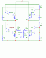
But I suggest you reference the mosfet drive power supplies to the sources of the mosfets being driven, like shown in my diagram. You should be able to add as many windings to the transformer as needed to derive those voltages. Be sure they are regulated to no more than the voltages driving the original mosfets. However, you do not need the biasing diodes I included in my diagram between the bases of the buffer emitter followers for your application. Be sure to take the drive signals for the new mosfets before the gate resistors of the original mosfets. Is the diagram here like what you are doing?
I am glad you mentioned the gate resistors, the importance of which I failed to mention. I think I see what you are doing.
Sounds like you are going to make quasi H-bridge and you are constructing buffer emitter followers whose bases will get their signal off the drivers for the two mosfets there already. Those two pairs of transistors will then drive the two new mosfets via suitable gate resistors. Sounds like a good idea and quite feasible.
But I suggest you reference the mosfet drive power supplies to the sources of the mosfets being driven, like shown in my diagram. You should be able to add as many windings to the transformer as needed to derive those voltages. Be sure they are regulated to no more than the voltages driving the original mosfets. However, you do not need the biasing diodes I included in my diagram between the bases of the buffer emitter followers for your application. Be sure to take the drive signals for the new mosfets before the gate resistors of the original mosfets. Is the diagram here like what you are doing?
Attachments
The dead time is done at the LM4651, I assume that transisters wouldn't have this problem since they don't have a gate capacitance.There are many interrelated issues here. The switching freq itself is not as critical as the switching speed. You want to switch the fets fast to avaoid losses, say within 100nSec? (I'm no expert on this, will readily yield to an expert). Then also it is IMPERATIVE that you avoid that both fets are on at the same time because that is a dead short across the supply, probably blowing the fets to smithereens. So you need what is called dead-band: the on-fet switches off, and a small delay later the off-fet switches on.
the bipolar stage here is what i'm getting at, except replace the transisters with higher spec'd ones where neccesary and raise the Vcc to 10v above rail. One question is with the fet on the negative supply would te source voltage be 0v (using n channel's) and the drain would be at the negative rail voltage? this would make the voltage needed to switch it on 10v?
Thanks all for your comments
Very much Appreciated
This is still buggin me coz I havn't fully got it sorted yet
The main part of the ESP schematic I was refering to was Q1.2.3.4 and M1,2,3,4.
My plan was to instead of the pulse from the 3525 the class D chip signal would be fed to the bipolars. Q1 would have VCC + 10v (in this case 57v) instead of 12v and Q2 would remain grounded. The signal being fed to the base of both bipolars would be the 25v.
disregard the rest of the schematic but the bipolars, mosfets and resistors between.
The total gate capacitance would be ~11nf so most, if not all, mosfet driver IC's are ruled out.
also in regard to transistors, what does it take to fully turn them on?
fr0st said:The signal being fed to the base of both bipolars would be the 25v.
Ok, you lost me when you got to this statement. Do you mean 0 to 47 volts switched high and low?
also in regard to transistors, what does it take to fully turn them on? [/B]
They amplify the current applied to the base, up to point. The gain drops as the current gets higher to where it eventually drops to one. But that can only be for a short burst, like charging and discharging mosfet gates. otherwise they will blow.
You can get faster switching times by using low voltage transistors and bootstrapping their power supplies so that the NPN collector always stays just 12 volts above the source of the upper mosfet as it turns on and off, it pulls the power supply for the emitter follower pair (both NPN and PNP) with it. Every time the the lower mosfet turns on it pulls the source of upper mosfet low and a diode connected to the lower 12v supply charges a capacitor for the supply which floats with the upper mosfet and is referenced to its source. Like how the upper power supply is gotten here.
http://www.irf.com/product-info/datasheets/data/ir2110.pdf
The MC34151 would be good apart from its only a low side driver. The main problem with this sort of thing is that you need 10v above the high rail (e.g 60 of a 50v rail) to turn the fet fully on, the 2010 would be perfect if I wasn't trying to drive so many fets
Is there any chance that your able to reference me to a discrete version of what your describing, from the descriptiong I can't quite figure out how it all fits together.
The high/low signal coming from the PWM chip is 0 to 25v.Ok, you lost me when you got to this statement. Do you mean 0 to 47 volts switched high and low?
Is there any chance that your able to reference me to a discrete version of what your describing, from the descriptiong I can't quite figure out how it all fits together.
OK, I will try to help you with bootstrapping and how you can use the IR2110 to drive as many mosfets as you like. This schematic can be seen at my web-site in my signature.
I solder the IRF7343 directly onto the ir2110. It is the only SMD I use. It has very low channel resistance figures for both its mosfets in its SO-8 package.
D1 and C1, the .22uf monolithic or tantalum may have be increased in value if you're driving much more gate capacitance than 10000 nF. The IRF7343's are configured as source followers, so they do not waste any power while switching.
Attachments
I've been heavily looking into how the whole process works and it turns out the LM4651 would be useless for the task due to its mosfet drive already in it.
With a little more research I'm planning on using a digital PWM processor and A/D converter to generate a logic level PWM pulse fed to an IR2010 or similar.
One concept I havn't yet benn able to figure out is how the IR2010 would work in a split rail H-bridge rather than having the low side grounded. so I've got a few more questions
what is the bootstrap cap charged to (voltage wise)? and what is it reference to?
I imagined it was charged to Vcc so when the positive side was refenced to the gate the Fet saw a 12v difference between the gate and source but this is probly wring since the cap would have no way to charge since the Vs pin only ever see's the high rail. (if that makes sense).
Also is the IR2010 capable of putting out a -40v as a gate drive or will if use a bootstrap topology again?
thanks subwo1, your definately being very helpful!
did you look at this page:
here's a link to IRF's recommended MOSFETs for the IR2010 controller in audio applications:
http://www.irf.com/product-info/audio/fsaudio.html
here's a link to IRF's recommended MOSFETs for the IR2010 controller in audio applications:
http://www.irf.com/product-info/audio/fsaudio.html
Hi fr0st,
Well, for one thing, if you use split rails, you do not need a full H-bridge. You can still do that with no problem if you want to by simply placing all the control and logic circuitry on the negative rail where the IR2010 is referenced. You will need two IR2010's with signals on the input pins 180 degress out of phase with each other, and then take the output across the mosfet totem poles.
With split rail power supplies, you have the option of using the simpler setup of the half bridge. You can take the output between the totem poles and connection between the upper and lower supplies. But either way your IR2010 has to be at the lowest voltage location.
It sounds like what you really want to do is use a single polarity power supply with your control circuitry at ground potential, the bottom, and take the output from a full bridge, or H-bridge, as it is also called.
The bootstrapping is a good thing. It makes it so much easier to drive the upper mosfet. The VSS pin is actually pulled low when the lower mosfet is turned on. Of course, the upper one had better be off at that time, or smoke! Then, when the IR2010 turns on the upper mosfet, using its source pin, carries the bootstrapped power supply up with it. I did not see on the data sheet that the IR2010 uses internal logic to prevent both outputs from turning on at the same time, but I am aware that the IR2110 and the IR2113 do.
I was looking at circlotrons schematic of his output stage and it all clicked!
His output drivers where actually using the negative rail (-50v in his case) as the ground, so the drivers where powered off -35v to get the 15v potential difference. By referencing the speaker to the true ground it creates the postive/negative voltage swing
I'm guessing this means that all digital circuitry that I use will have to be reference to the -50v rail so I need to regulate the 0v (+50v when reference to the -50v line) down to whatever I need?
EDIT: I just looked at the IR2110 datasheet and it has seperate grounds and Vcc for the logic and switching sides which answered my question for me
His output drivers where actually using the negative rail (-50v in his case) as the ground, so the drivers where powered off -35v to get the 15v potential difference. By referencing the speaker to the true ground it creates the postive/negative voltage swing
I'm guessing this means that all digital circuitry that I use will have to be reference to the -50v rail so I need to regulate the 0v (+50v when reference to the -50v line) down to whatever I need?
Would using an IR2110 remove the need for adding dead time?I did not see on the data sheet that the IR2010 uses internal logic to prevent both outputs from turning on at the same time, but I am aware that the IR2110 and the IR2113 do.
EDIT: I just looked at the IR2110 datasheet and it has seperate grounds and Vcc for the logic and switching sides which answered my question for me
The seperate grounds betweem the driver and logic on the 2110 have the constraint that the grounds are not allowed to separate by more than 5V. Sometimes they are connected by a 1ohm or so resistor to help isolate switching spikes. But so far, I have always tied them directly together.
peranders said:I have read this thread but I haven't got the whole picture.
10 kVA in a car with 12 V? = 833 A!
How much power do you want and what loudspeaker impedance do you have?
How much I and U must the SMPS be able to deliver?
The whole thing (class D amp + SMPS) will never be run @ 8kw (max amp spec) for longer than an SPL burp (usually 3 sec). Thats loaded down to .5ohms. It unlikly that I'll get speakers to do that for a while but its surpose to be a competition amp.
Sofare I have 20 75amp,60v Fet's for the SMPS (onsemi's ones) and 20 52amp,100v fets for the output stage. Ti have 9 amp driver which i'm going to use for the SMPS but the amp's output needs a high side driver with a high amp rating to get a decent rise/fall time.
If I parrallel the IR2110's will it affect the rise/fall times of the PWM chips logic output? (seperate bootstap caps)
It might turn out simpler than to add an extra Fet stage.
- Status
- This old topic is closed. If you want to reopen this topic, contact a moderator using the "Report Post" button.
- Home
- Design & Build
- Parts
- Switching Large amounts of FETs