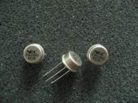
I have bought some 2SK1383 Transistors and then i will test its.
This device is a SIT transistor one sort of V-fets or vertical Jfet.
I not found the datasheet for its and i have thought to test its with digital multimeter.
Against in my mind its behaviour are different from common jfets.
N jfet for example present a PN junction of 0,5 V between Gate- source and gate-drain (positive tester on gate) and a resistance from 20 to 100 Ohms between source and drain about in both direction.
Indeed testing 2SK1383 i have found one junction voltage of 0,517 V between two terminal (I not know for sure the pins of 2sk1383). So I think that the pin on the + terminal tester is the gate and the other two terminals are the drain and the source.
But when i test among these last, i not read low resistance as jfet but high resistance or open circuit. All other configuration results as open circuit, so i have doubt on the effettive pins assignaments or at the end if this devices is a real SIT.
There are anybody that can help me?
Thanks, Francesco
Hi, Francesco,
After researching this transistor further I am afraid that this
transistor may be not good for audio: it is SIT, but not V-FET.
It looks like a BSIT - SIT with bipolar type of characteristics.
It will require gate current to be conductive between drain
and source.
Its Vgsmax is 5 V, with negative Vgs it will be OFF. For conduction
it will need regular ~+0.6 V Vgs.
Its pinout looking at the bottom is: D G S-near case key
These BSITs are intended for switching applications - with gate
current their channel Rds will be significantly reduced - like for
any JFET (although BSIT will not have "any" Rds to start with).
In this bipolar mode they will have good switching characteristics,
but Beta (Id/Ig) may be highly nonlinear, droping severely with
increased current. Considering everything, they may not be
a competition to a good bipolar npn drivers.
But, check what kind of Ids=f(Uds) characteristics these
transistors will have with the different Ig: triode or pentode?
Steven
thanks much Steven for your reply.
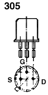
Looking to the attached figure for the package and Pin of 2SK1383 that i have found, i measure P-N junction between S and D. So i think this figure isn't correct or i am in error?
However if you are right, then i must biasing this device as a mosfet? (gate positive respect to the source).
Just I would to feel if the output characteristics are triode-like.
I have spent many time to find one SIT device good for audio
especially for signal or medium power type.
Francesco
Attachments
Other specs about this devices i have found in:
http://www.datasheetarchive.com/2SK1383-datasheet.html
If I remember Bsit means bilateral SIT that's it can be employed in depletion or enhancement mode.
However also the Lovoltech LU1014D are for switching not for audio but Nelson Pass have built many great audio amplifier, althought its VDS max is 5 V.
This is why i hope to employ this device.
Francesco
<Looking to the attached figure for the package and Pin of 2SK1383 that i have found, i measure P-N junction between S and D. So i think this figure isn't correct or i am in error?>
All these databooks do have errors (human error), so don't be
surprised if it will turn out to be different from the pic.
<However if you are right, then i must biasing this device as a mosfet? (gate positive respect to the source).>
Yes, but think of it not as mosfet, but regular npn bipolar transistor.
And find the gate (+) that will check as a "diode"
(on your DMM) to Source(-). The last pin will be Drain.
Contol the input current, not the voltage.
<If I remember Bsit means bilateral SIT that's it can be employed in depletion or enhancement mode.
However also the Lovoltech LU1014D are for switching not for audio but Nelson Pass have built many great audio amplifier, althought its VDS max is 5 V.
This is why i hope to employ this device.>
There is no such thing as bilateral SIT. BSIT stands for SIT with
Bipolar transistor behavior - pentode output characteristics, gate
current needed to work. Only one mode of operation. This is, what
I suspect, you have.
Lovoltech are SIT and V-JFET (that is the type you are looking for).
While it was developed for switching applications, it can be used
for audio amplification. (It has at least 20 V Vdsmax, right?, but
still not enough to take advantage of it's low output impedance
and to produce enough Drain voltage swing).
So, try to make the necessary measurments to see what do you
have.
Sorry for the mistake: BSIT means Bipolar Sit as you report.
But in the above attached file, the type of device for the 2sk1383 is SIT not BSIT as you suspect. What is your font?
I can tell you another url:
http://esapub.esrin.esa.it/pss/pss01603/p1_12_05.htm.
Turn to the figure 305 and agree with my measure the PIN must be: G - D - S
Next day i polarize it as a NPN transistor as you advice me.
Precious information to begin this work.
Thanks, Francesco
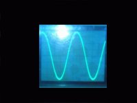
Hi, today i have try to work with this device. See the attached image
After any tentative this is my result:
1) the PIN assignament in figure 305 (above) is correct
2)VGS must be positive as MOS or NPN BJT
3)There is not current to flow trought the gate (like Mos)
4) with VGS=0 flow little current in the Drain circuit, so, i think, it go off for negative Vgs
5) the Drain current begin to rise for Vgs > 6 mV
Then i have applied a sine signal generator to view the outuput waveform. The upper side is squeezed the down side is prolonged. Remember the Mos type.
With high Drain current and low RC the form is a little better.
Francesco
Attachments
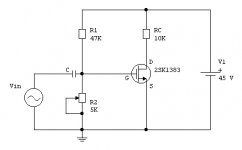
I will post image of schematic for measure gate current.
I have biased the gate for a voltage drop on Rc=20 V.
When i have put in circuit RB (10k) the voltage drop on RC stay the same. Then, for great surely, i have measured in Volt the drop voltage on RB and it was zero. So there is not current absorbition by the gate.
Francesco
I have biased the gate for a voltage drop on Rc=20 V.
When i have put in circuit RB (10k) the voltage drop on RC stay the same. Then, for great surely, i have measured in Volt the drop voltage on RB and it was zero. So there is not current absorbition by the gate.
Francesco
Attachments
Thanks Steven for you suggestions.
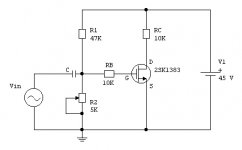
Today i would investigate better the point number 4 (little drain current with Vgs=0) to view if it working also a normal JFet.
To make that i have realized the little circuit as attached
Yes it work, also with negative Vgs (autobias), but the better performance in linearity is around 14V of Vds, so on RC must be drop 26 V.
If I want that it work as JFet the major Drain current is for Vgs=0.
Very interesting this point, i can eliminate the RK and CK other the input capacitor. I think that the input network for a signal is very very important: this is a big advantage to put off capacitors and resistors.
However the RC is very high:470k, and the bandwith is narrow.
Distortion in very low, up to output voltage=5,7 Vrms for a relative input signal=304 mV (Gain good a this low current).
Thanks, Francesco.
Attachments
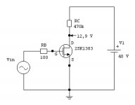
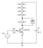
Hi, next step a will understand if this device work as a regular SIT or no. To make that i have splitted the RC (470K) in 4 resistors of 100K plus one of 62K as the schematic below. i Have put in fixed mode the DMM among RC5 to view the voltage drop so at the end the drain current and have shunted each times the other RC resistors. This is the result:
Resistor shunted V on R5
nothing 3,79 V
RC1 3,82 V
RC1+RC2 3,85 V
RC1+RC2+RC3 3,87 V
RC1+RC2+RC3+RC4 3,90 V
The result show the drain current substantially fixed enough as a mos or jfet not as SIT in my idea.
Let me know yours.
Thanks Francesco

Resistor shunted V on R5
nothing 3,79 V
RC1 3,82 V
RC1+RC2 3,85 V
RC1+RC2+RC3 3,87 V
RC1+RC2+RC3+RC4 3,90 V
The result show the drain current substantially fixed enough as a mos or jfet not as SIT in my idea.
Let me know yours.
Thanks Francesco
Attachments
Last week, i have tried to use this devices as last power device in a little push-pull amp.
For this work i have put the 2SK1383 in my one stage push-pull amp in place of IRF530. It work well, more bass, a little bit extended high, peraphs a better microdynamics and resolution.
On a load of 8 ohm max clean output voltage was 6,5 Vrms so output power was about 5-5,5 W.
I think to name it Baby-Sit
I think It should work good also in similar headphone amp
These devices have an high positive current thermal coefficient.
By the way a special system to fix this on a great heatsink was neeed.
I will post images as soon.
Francesco
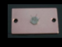
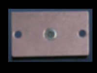
Today i will post images relative to 2SK1383 used in power stage.
Because it product hot temperature, then it was necessary to couple it with great heatsink in unconventional mode. Before in a copper bar 20x50x4 mm ca was realized one hole (d=8 mm), then this bar was fixed to heatsink with two screws. Between bar and heatsink there is a mica foil and silicon grease. In the following the images for this work (excuse me for poor quality).
Francesco
Attachments
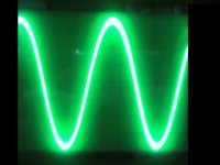
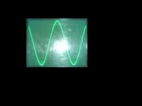
Last image is for sine signal image obtained in my scope.
F=1 KHz
V/div=2 Volt
T/div=2mS.
As you can see it's a beautiful sinewave
The amp work with no feedback overall, but only 0,22 Ohm source resistor for least control against temperature runway.
Francesco
F=1 KHz
V/div=2 Volt
T/div=2mS.
As you can see it's a beautiful sinewave
The amp work with no feedback overall, but only 0,22 Ohm source resistor for least control against temperature runway.
Francesco
Attachments
- Status
- This old topic is closed. If you want to reopen this topic, contact a moderator using the "Report Post" button.
- Home
- Design & Build
- Parts
- static induction transistor identity pins