I think that the easiest and best way is with the photo-sensitive PCB material. I can get trace width of 8 mils repeatedly. I print to over-head transparency material, expose on a photographic light-box, develop in dilute NaOH and etch in a cocktail of H2O2 and HCl.
There's a very good PCB user group on Yahoo --
I have done small PCB's with non-photosensitive material directly on an HP7475A plotter. Anything greater than about 4 square inches has too much mass to use a plotter. You can then trance over the plotted lines with a waterproof sharpie.
There's a very good PCB user group on Yahoo --
I have done small PCB's with non-photosensitive material directly on an HP7475A plotter. Anything greater than about 4 square inches has too much mass to use a plotter. You can then trance over the plotted lines with a waterproof sharpie.
And there is allways Press N Peel ,I get quite Thin and consistant Traces useing PNP even though I allways try to keep the Traces and pads as Fat as possible in the space allowing but when building things like active electronics for guitars you sometimes have to make a curcuit fit on a 1sq in Area or smaller....
I have also had very good results just useing my Lazer printer to print on to Magazine paper ,It also gives quite good results ,allmost as good as PNP.....
also another tip is instead of useign expensive etchant like Amonium persulfate or ferric chloride you can save a lot of money and even time useing a mixture of 2 parts hydrogen Peroxide with 1 part muriotic acid ,I find this is the Fastest and cheapest etchant arround, just don"t breathe in the fumes or get it on your skin......
Good luck
jackinnj said:I think that the easiest and best way is with the photo-sensitive PCB material. I can get trace width of 8 mils repeatedly. I print to over-head transparency material, expose on a photographic light-box, develop in dilute NaOH and etch in a cocktail of H2O2 and HCl.
There's a very good PCB user group on Yahoo --
I have done small PCB's with non-photosensitive material directly on an HP7475A plotter. Anything greater than about 4 square inches has too much mass to use a plotter. You can then trance over the plotted lines with a waterproof sharpie.
But then come the FUN!!!..Drilling the result. I have trouble keeping the small carbide drill bits from breaking .....Anybody got a system for successful drilling???


davidallancole said:Minion, have you found that the 2 parts hydrogen Peroxide with 1 part muriotic acid needs to be heated 10-20 degrees above room temperature to make it work good? I found that it was utterly slow at room temperature.
Actually I haven"t had that problem ,I use it at room Temp and I actually notice that the Chemical reaction happens right away and starts to create it"s own Heat....It takes maybe 5 min for a Small PCB (3 in SQ) and maybe 10 min for a large one(6+ in SQ)....
The trick is to keep agitateing the Acid mixture ,I usually put the acid and the PCB in a sealed Plastic baggie and put that in a tupperware container with an air tight lid and just shake it for a few minutes and it is done ,I also get a faster etch if I put a bit more acid in the Mixture.....
Cheers
Drilling made easy...
Hi,
i use a Drill Stand like this one:
http://www.minicrafttools.com/28606.html
works 100%, easy to use, and no broken bits...
Michael
Hi,
i use a Drill Stand like this one:
http://www.minicrafttools.com/28606.html
works 100%, easy to use, and no broken bits...
Michael
Re: Drilling made easy...
Thanks .... maybe I could send the bits and boards to you and wind up with Boards made In Vienna .... I'm getting so old my hands dont work anymore.....seems everything goes wrong.
atarashi said:Hi,
i use a Drill Stand like this one:
http://www.minicrafttools.com/28606.html
works 100%, easy to use, and no broken bits...
Michael
Thanks .... maybe I could send the bits and boards to you and wind up with Boards made In Vienna ....
I'm getting so old my hands dont work anymore.....seems everything goes wrong.You can go for photosensitive pcb but the trick is the proper contact of the mask on the board. I use g-gramps with a home made exposure box.
Etching : ferrichloride is used you will find all you need for etching for quite cheap...guess where fish aquarium shop. Air pump + aquarium heater will do the job and they sell the plastic tubes you need.
Developping: tried caustic soda its bad am using sodium hypochloride it develops great within seconds.
Try doing each step one by one until you get good results. Tiem, required, amount and concentration of solution is important easiest is to try with small pieces of pcb until you get each step right
Use the high speed steel bits and throw them out when they get dull.sandstorm33 said:But then come the FUN!!!..Drilling the result. I have trouble keeping the small carbide drill bits from breaking .....Anybody got a system for successful drilling???
I used a Ryobi in a Dremel Press -- i have a block of balsa wood underneath.
I can also drill PCB material with Carbide bits in my Grizzly Mill -- but you need to get the correct collets -- and the bit can't be subject to any horizontal pressure. You can often find the carbide PCB bits (used) on EBay.
Save your time, use your wallet, just buy some press 'n peel
From the lazer printer to the board to the etch.. 3 simple steps a retard with one arm could do...
Photoetching these days just gets me in all the wrong ways... I am sure with all the right equipment from lights to timers the balance shifts in favour of phototechniques, but I am tired of the inconsistent results I got...
you don't need no airpumps, I put the stuff in an icecream tub and just swirl it around while watching some tv for a few minutes until the etching is done... No fuss, no mess... those splattering staining bubbles will make me suicidal...
For handleing thin drill bits, invest in a pinvice, you put the bit in there, leaving only a few milimeters exposed to keep horizontal forces from breaking 'em, and then put the whole thing in the drill press...
 with your icecream tub in case you get thirsty
 It is about twenty rand... equivalent to say spending $2 or 1 gpb = allthough not equal just relative value....
You learn to be very resourcefull... printing small boards on a piece of paper to mark the spot, then tapeing just enough P 'n P over it to cover it, then take the funny sheet to the print shop (I don't have a lazer printer or photocopier), they give me a funny look but do it anyway as i look so sure about myself...
Yep the Fe cholride looks a bit luik guiness (but I'm not a drinking man anymore - maybe two or 3 beers and a glass of wine or two a year... stomach can't realy handle acid anymore. Don't drink Coke kids...
Agus Widarto said:Just Now I found from web site make PCB with Positive 20. can you tell me about Positive 20 ? this a brand merk or name of chemical..
Thank! for all your replay.
positive 20 is a spray on photoresist. I find that it is much better to use this spray than to buy the presensitised boards. The spray is a lot more forgiving on bad negatives and poor exposure times.
If your using positive 20 here is my advice.
1. Use cif or similar abrasive liquid cleaner to clean the copper board of all grease and surface corrosion. Dry with a lint free cloth.
2. Put on the oven (yep, the one in your kitchen) to about 75c allow this to heat up
3. spray on reasonably generously onto precleaned copper blanks.
4. Switch off the oven and put in your boards to dry in the heat. You can repeat if your doing 2 sided. give them about 15 minutes in the residual heat of the oven
I tried origionally to cover the sprayed boards and let them dry naturally. Never got good results. Dust always seemed to get in somehow no matter hoy clinical I thought I was being.
Positive 20 defo gets my vote for ease of use. It may seem more effort than buying presensitised boards, but was less effort than making mistakes.
I've done tape on mylar, to graphic arts film, with photo resist and FeCl. Ah, the good old days, what a PITA, and I was a photo darkroom buff. Then I tried direct writing by passing the boards through my HP pen plotter. That worked too, but the resist ink wasn't durable enough. Then I started doing iron-on from plain old laser printer prints on various photo papers. That's actually the winner for home use. High quality and great resolution. No really special materials are needed, but not that many people have a laser printer these days- ink jet has taken over. Today I don't bother with any of it. I just bite the bullet and send my CAD files to AP Circuits (or the vendor of your choice). Two days later my professionally made boards arrive, plated thru, drilled, and ready to go. If your time is worth a nickel an hour, great, make your own boards. Otherwise, spend the time doing something profitable and let the board house do the work.
BTW, the one exception is when I need something simple, fast. Then I pencil the layout and just cut the copper with a Moto Tool and a carbide burr.
BTW, the one exception is when I need something simple, fast. Then I pencil the layout and just cut the copper with a Moto Tool and a carbide burr.
originally posted by justblair
I find that it is much better to use this spray than to buy the presensitised boards. The spray is a lot more forgiving on bad negatives and poor exposure times.
I had opposite experience.
First, it`s hard to clean copper really well as it oxidizes in no time.
Second, it is also not so easy to apply the spray as evently as is the coat on the ready made precoated PCBs. When the photoresist layer is not applied evenly the potentially advantage regarding bad negatives and exposure time is gone.
Third, the PCB has to be completley dust free prior to coating, otherwise even the smallest particles will cause errors. This may or may be not a problem depending on the intended application and the desired resolution of the board.
Quality precoated PCBs cost only a few cents more.
IMO it isn`t worth to hassle with photoresist laquer oneself.
I find that positive presensitized PCB and inkjet transparencies are the easiest method. However, the four steps of the process should be done with great care because once something has gone wrong in one step you will have serious trouble to get the following steps right. On the other hand, good transparencies give a better error margin for UV exposure time. Optimum UV exposure time gives a good error margin for NaOH concentration in developer solution. Optimum developing results in almost fool-proof etching...
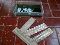
Double sided DIY boards are easy to do...
This is an envelope-like transparency. There are two inkjet transparency sheets on each side, with the ink facing the inner gap to avoid being scratched. All the layers are carefully matched and firmly held in place with tape. The heavy ink load will act as a glue and wiill further keep the two sheets of each layer stuck. The PCB is placed inside the "enveloppe" during UV exposure to guarantee matched patterns at both sides. Care must be taken to avoid the PCB moving when a single side UV exposure system is used and the PCB is turned over to do the other side.
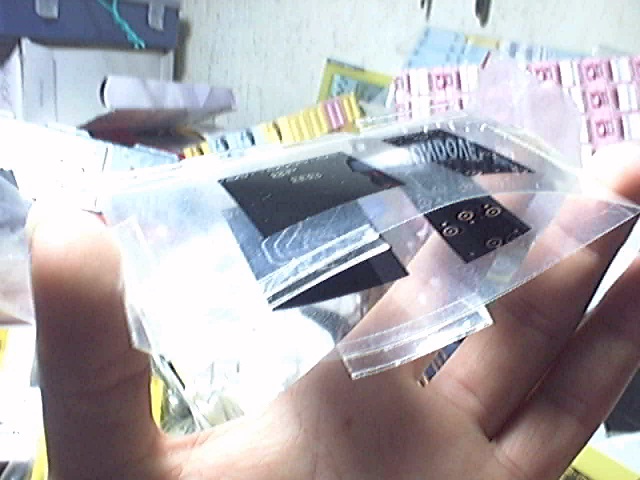
This is the PCB once developed and etched. Note the bent corners trick in order to force some spacing between the board and the bottom of the tanks and avoid scratches during developing and etching.
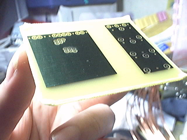
This is the the other side. The green coating is the remaining positive photo-sensitive layer. I don't remove it as it's quite efficient in preventing copper from corroding and it has good solderability.
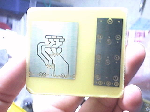
Now it's time for drilling and cutting...
BTW: The skin of my hands is now complaining about the chemicals Fortunately I do DIY PCBs once every week or two at best and I do the etching outdoors with plenty of wind to avoid fumes. The amount of money and time saved in prototypes is substantial.
This is an envelope-like transparency. There are two inkjet transparency sheets on each side, with the ink facing the inner gap to avoid being scratched. All the layers are carefully matched and firmly held in place with tape. The heavy ink load will act as a glue and wiill further keep the two sheets of each layer stuck. The PCB is placed inside the "enveloppe" during UV exposure to guarantee matched patterns at both sides. Care must be taken to avoid the PCB moving when a single side UV exposure system is used and the PCB is turned over to do the other side.
This is the PCB once developed and etched. Note the bent corners trick in order to force some spacing between the board and the bottom of the tanks and avoid scratches during developing and etching.
This is the the other side. The green coating is the remaining positive photo-sensitive layer. I don't remove it as it's quite efficient in preventing copper from corroding and it has good solderability.
Now it's time for drilling and cutting...
BTW: The skin of my hands is now complaining about the chemicals
Fortunately I do DIY PCBs once every week or two at best and I do the etching outdoors with plenty of wind to avoid fumes. The amount of money and time saved in prototypes is substantial.- Status
- This old topic is closed. If you want to reopen this topic, contact a moderator using the "Report Post" button.
- Home
- Design & Build
- Parts
- To Make Good PCB at home