They'll work with Vcb=0, but it would be better to put something (diodes/LEDs/other) between the emitters of Q6 and Q9 and the rails to provide some extra voltage drop. Especially if the mirror is degenerated, as it should be.
You could put small signal diodes in serial with the relevant
collector of the current mirror , this will increase the VAS
base voltage by 0.65V and allow to degenerate it with enough
voltage drop in the degeneration resistor to provide DC current
stability.
Problem , wich already exist without those diodes but in a lesser
extent , is that the VAS base emitter capacitance cant be
discharged fully.
Attachments
Last edited:
Sorry, I don't follow. Where is gain being lost?
A saturated transistor is not much of a load for the input jfets, to rely on any significant open loop gain in the input stage. To add insult to injury, probably most of the harmonic distortion cancellation due to the current mirroring effect is lost.
The feedback loop(s) are loading the VAS with about 550ohm and if you consider 100 ohm emitter degeneration it won't allow a VAS gain over 11 (550ohm/50ohm).
One to another the open loop gain will be low, probably under 20dB at LF. Output impedance is 50ohm, nothing to call home about. Also, your VAS bias is dependent on the jfets Vp, which in turn is temperature dependent, has rather large device and batch dispersion, etc...
There are ways to make this topology work properly, but nothing that would not further add to the complexity (or further trade the performance).
To continue.
The reason I design like this is to do three important things:
1. To linearize the inherent nonlinearity of the solid state devices.
2. To remove the need for either input or output coupling caps.
3. To allow the complementary drivers to drive each other, rather than some parasitic load resistor, especially when maximum voltage swing is encountered.
This minimizes the change in current with voltage swing, lowering distortion. Also the complementary drivers each add to the signal output, cancelling even harmonics and reducing the burden on any one active device.
However, to keep open loop gain up and 'noise insertion' from active loads down, resistors are almost always used as load resistors for the first stage.
Enough for now.
Last edited:
You could put small signal diodes in serial with the relevant
collector of the current mirror , this will increase the VAS
base voltage by 0.65V and allow to degenerate it with enough
voltage drop in the degeneration resistor to provide DC current
stability.
Problem , wich already exist without those diodes but in a lesser
extent , is that the VAS base emitter capacitance cant be
discharged fully.
I am again really surprised on how much confusion this topology is creating. No, I don't your topology would work outside the simulator, other than by accident, and with the known thermal issues.
Can you tell, by inspecting the schematic, how much is the voltage in the Q9 base? Hint: no, it is ill defined.
At least, Godfrey schematic tries to define the VAS bias by using the input stage differential bias voltage (about 2Vp) divided by the VAS collector resistor. This one is, bias wise, practically identical to the Slone's fig 11.4 famous blunder.
A saturated transistor is not much of a load for the input jfets, to rely on any significant open loop gain in the input stage.
Just a fine point, 0 Vcb is not saturation ~0 Vce is. If you check schematics IC's are packed with devices operating at 0 Vcb. Many single supply op-amps with pnp inputs operate fine with the inputs 200mV below -V (gnd).
Just a fine point, 0 Vcb is not saturation ~0 Vce is. If you check schematics IC's are packed with devices operating at 0 Vcb. Many single supply op-amps with pnp inputs operate fine with the inputs 200mV below -V (gnd).
True, saturation is defined by forward biased BE and BC junctions. As Vcesat can be like 100mV, Vcb needs to be < 0 (~-0.5V) for true saturation. Vcb=0 would be closer to quasi-saturation (don't know in discrete bjts the intrinsic BC potential). Anyways, Vcb=0 is a shaky situation for a discrete design.
There could be a semantic element to this, I meant saturation as the inflection point where things stop working. Considering the simplest current mirror, the diode connected transistor has 0 Vcb by definition and at 0 Vcb for the second transistor there is no degradation of the current mirroring (i.e. gain).
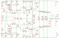
Well I got self-snookered into looking at this, my own damn fault. I've tried to preserve most of the "locally original" simplified schematic, and various versions get progressively better, the attached being one of the later ones. Given that the cascoding is taking away a few volts I suppose a better I mirror could lose a little more, but for better or worse they remain the simple ones and have ~0 Vcb.
Thermal compensation has been done for the second stage devices, imperfectly primarily because the common-base ones have significantly different voltage swings at their emitter. The base bias 3V sources are left as an exercise. If provided by another complementary transistor the cascodes could be made Boxall (aka Larson-Baxandall) cascodes, with all of their attendent potential for headaches")
The notion here is to servo one half and let overall closed-loop feedback take care of the other half. I make no claim as to how big of characteristics spreads are accomodated by the modest amount of correction from the error amplifier --- this is not a design presented as ready for production. The 300mV reference sets the output stage standing current to about 30mA.
The input devices are cascoded for smaller dissipation shifts with signal swing. I simmed with ideally matched SK170s and SJ74s, not the dual parts shown, and of course the cascode devices are identical too.
I'm not enthusiastic about this, and one can see how it gets complex in an attempt to make it better-determined. But it probably can be made to work adequately. Sweet Spice lies are shown as annotations.
Thermal compensation has been done for the second stage devices, imperfectly primarily because the common-base ones have significantly different voltage swings at their emitter. The base bias 3V sources are left as an exercise. If provided by another complementary transistor the cascodes could be made Boxall (aka Larson-Baxandall) cascodes, with all of their attendent potential for headaches
The notion here is to servo one half and let overall closed-loop feedback take care of the other half. I make no claim as to how big of characteristics spreads are accomodated by the modest amount of correction from the error amplifier --- this is not a design presented as ready for production. The 300mV reference sets the output stage standing current to about 30mA.
The input devices are cascoded for smaller dissipation shifts with signal swing. I simmed with ideally matched SK170s and SJ74s, not the dual parts shown, and of course the cascode devices are identical too.
I'm not enthusiastic about this, and one can see how it gets complex in an attempt to make it better-determined. But it probably can be made to work adequately. Sweet Spice lies are shown as annotations.
Attachments
Hi,
You are putting the diodes into the wrong line.
Let the CM Transistor carry the voltage, it needs it for high impedance (I'd say give it at least 3V), put extra diodes in line with your VAS to up voltages if needed...
Actually, Robert C shows how this can be made to work in his book.
Actually, I have not been giving RC his dues.
I find his book is well worth what I paid, even ten times than what I paid (with DS's books I always feel they are worth 1/100's of the cover price but I buy them anyway and then feel cheated).
Now past that, the only reason to use CM on the IPS is to maximise looped negative feedback and to maximise the impact of the non-ideal behaviours of the next stage on the systems linearity.
Someone please remind why exactly would I want to do something so monumentally devoid of intelligence, apart from DS's say so?
CM load has it's uses and places, but maybe not there...
Ciao T
You could put small signal diodes in serial with the relevant collector of the current mirror , this will increase the VAS
base voltage by 0.65V and allow to degenerate it with enough
voltage drop in the degeneration resistor to provide DC current
stability.
You are putting the diodes into the wrong line.
Let the CM Transistor carry the voltage, it needs it for high impedance (I'd say give it at least 3V), put extra diodes in line with your VAS to up voltages if needed...
Actually, Robert C shows how this can be made to work in his book.
Actually, I have not been giving RC his dues.
I find his book is well worth what I paid, even ten times than what I paid (with DS's books I always feel they are worth 1/100's of the cover price but I buy them anyway and then feel cheated).
Now past that, the only reason to use CM on the IPS is to maximise looped negative feedback and to maximise the impact of the non-ideal behaviours of the next stage on the systems linearity.
Someone please remind why exactly would I want to do something so monumentally devoid of intelligence, apart from DS's say so?
CM load has it's uses and places, but maybe not there...
Ciao T
Hi Brad,
Sure, it will work. But do we really need the CM?
If we must have high impedance loads (which I'd question), there are ways that do not carry DC stability penalties (bootstrap instead of CM).
Ciao T
Well I got self-snookered into looking at this, my own damn fault.
Sure, it will work. But do we really need the CM?
If we must have high impedance loads (which I'd question), there are ways that do not carry DC stability penalties (bootstrap instead of CM).
Ciao T
Hi Brad,
Sure, it will work. But do we really need the CM?
If we must have high impedance loads (which I'd question), there are ways that do not carry DC stability penalties (bootstrap instead of CM).
Ciao T
No, we don't. That's why I say I was snookered. The mountain I didn't see the point to climbing kept leering at me in my troubled sleep.
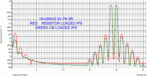
Here is the relative variation of the impedance modulus of various resistors with frequency. The vertical axis is |Z(f)| / |Z(200Hz)|, total span of the axis is +-2%.
Even at medium frequencies there are some ripples of impedance (possibly some electrostrictive deformation).
These results are taken at the same 1V RMS test sine signal. Impedance will also vary by the test signal amplitude variation. I am afraid to imagine what goes on with a given resistor when unstable schematics usually oscillate (10...100MHz).
Constructional aspects into higher impedances (resistor value) at higher frequencies creating capacitive flashover. ie the complex LCR of the materials comes notably into play at the higher 'resistor value impedances'.
IMO, high delta or high V/s will also achieve the same effect. (hopefully that's a 'duh!' statement)(high V differential across the given resistor will also encourage the condition - more 'duh!')
There are ways to deal with this.
Last edited:
Still would benefit from cascode in output. These circuits get so linear that the Vas non-linear Ccb can add even up to 20dB to the thirds at 10kHz
BTW the avatar is "woman ball player", the Mayan version of "ball" had unfortunate consequences for the loser.
Serious game. decaptiation and...thus.... 'new ball' (IIRC). Until the summer heat sets in, that is.
Like backwoods teenagers with their partridge feet they take to school to scare the girls (by pulling on the tendons and making the toes move). But at a slightly different level.
Last edited:
Brad,
As there is only one good reason to climb a mountain ("It was there") you are totally excused. Carry on Soldier.
Ciao T
No, we don't. That's why I say I was snookered. The mountain I didn't see the point to climbing kept leering at me in my troubled sleep.
As there is only one good reason to climb a mountain ("It was there") you are totally excused. Carry on Soldier.
Ciao T
Oh yes, there is something about the beauty of circuit drawn and imagined in engineers head and final sonic result. I've always believed in that.
Some airplane designer once said : "Only beautiful aircraft can fly".
The picture looks most like this p-diff & n-diff input combination that seemingly only
survives in self-acclaimed hi end audio.
Well, with regard to the airplanes, they said the Ka-8 glider airplane really doesn't fly,
but is repelled by the earth for being ugly. Nevertheless, it's very forgiving and a real
fun for beginners.
Gerhard
Last edited:
Brad,
As there is only one good reason to climb a mountain ("It was there") you are totally excused. Carry on Soldier.
Ciao T
Mount analogue Mount Analogue - Wikipedia, the free encyclopedia
The picture looks most like this p-diff & n-diff input combination that seemingly only
survives in self-acclaimed hi end audio.
Well, with regard to the airplanes, they said the Ka-8 glider airplane really doesn't fly,
but is repelled by the earth for being ugly. Nevertheless, it's very forgiving and a real
fun for beginners.
Gerhard
Hello Gerhard,
As they say, beauty is in the eye of the beholder. I see nothing wrong with KA-8. It flies by the forces of nature and one can not fool these with some marketing tricks... Have you tried it?
Here are some ugly ducklings:
20 World's most Ugliest Aircraft Designs Ever | Techxilla
Best,
Last edited:
I am again really surprised on how much confusion this topology is creating. No, I don't your topology would work outside the simulator, other than by accident, and with the known thermal issues.
Can you tell, by inspecting the schematic, how much is the voltage in the Q9 base? Hint: no, it is ill defined.
At least, Godfrey schematic tries to define the VAS bias by using the input stage differential bias voltage (about 2Vp) divided by the VAS collector resistor. This one is, bias wise, practically identical to the Slone's fig 11.4 famous blunder.
The confusion is in your brain , firstly...
Any moderatly trained eye will tell you that Q9 base voltage
is the sum of the diodes losses + Vce SAT Q9 + 1/2 tail current x R1.
Since the higher base voltage allow energic degeneration at the VAS
emitter , any CM unbalance is easily corrected by the global NFB
without unbalancing the VAS differential current.
Without this heavy degeneration the VAS current will be unbalanced
as a side will enter full conduction while the other one will be almost switched off.
Anyway , i built such an amp , although with a simple BJT VAS ,
not a darlington one as in the schematic above , and providing
minimal but not excessive components matching ;, it can be made
to work quite well.
You are putting the diodes into the wrong line.
Let the CM Transistor carry the voltage, it needs it for high impedance (I'd say give it at least 3V), put extra diodes in line with your VAS to up voltages if needed...
There s some advantage in implementing them this way...
The IPS has way better linearity with a CM , that s not onlyNow past that, the only reason to use CM on the IPS is to maximise looped negative feedback and to maximise the impact of the non-ideal behaviours of the next stage on the systems linearity.
Someone please remind why exactly would I want to do something so monumentally devoid of intelligence, apart from DS's say so?
CM load has it's uses and places, but maybe not there...
a matter of NFB maximization.
The reduction in IMD that it allow is simply stunning.
Attachments
- Status
- Not open for further replies.
- Home
- Member Areas
- The Lounge
- John Curl's Blowtorch preamplifier part II