I think you should look closer.
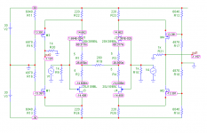
Both inputs have 4 transistors.
All common collector. In fact, there are two diamond buffers (unity gain buffers) and in between the 500 Ohm resistor.
In fact, in the left on the picture buffer currents powering an output pair of followers go directly to rails, in the right diamond buffer they go through current mirrors for amplification. Outputs of them are shorted through a current limiting resistor, such a way they are coupled.
Nothing common with 2 classical diffstages using JFETs where each other replaces corresponding current source in tail. Return tails back and nothing changes.
Tino, you are correct, it is the bipolar equivalent of the 4 quadrant jfet input stage. Wow, getting more primitive than ever!
No, it is not an equivalent of your 4-quadrant jfet input stage. Speaking of primitiveness, I never called your trick with eliminating of current sources in tails primitive; actually it is elegant. But what was your design target: an opamp (a device for instrumentations), or a preamp (a device for clean sound reproduction)? What is optimal for an opamp is suboptimal for preamp, and what is optimal for preamp is suboptimal for opamp. First of all, an opamp needs as less as possible DC shift. It is one of main design targets. Going for it in preamp you loose vital parameters, like S/N, linearity (I mean linearity with an order in mind since it is an audio linearity, not instrumental one), at least. Second, power efficiency. It is a second design criteria for opamps, that's why they are often made complementary. For audio it does not matter at all, especially in preamps! Going for it, you loose, the same S/N and (weighted for audio!) linearity.
You solved some problems, John. But you've solved wrong problems trading off real ones. That's what is called sub-optimality in design. Here I completely agree with Syn08.
Do you want to see some real examples of really optimal designs for audio? Go to PassLabs forum, and learn, learn, learn, then come back and let's discuss what you've learned...
Last edited:
Single JFET is primitive, with regards of cost/noise BT gain stage isn't optimal,
With regards linearity it is much linear than single device, with regards output current it doesn't exhibit symmetrical saturation as differential stage and asymmetrical saturation as single device. Intrinsic linearity of this stage allow you to use your loop gain to improve something else.
You are so full of it Dimitri, and the sad thing is that you know it

- Crap PSRR
- Crap CMRR
- Gain depends on load
- A textbook example on how to generate open loop PIM, both by driving the nonlinear MOSFET impedance and by driving the nonlinear output load reactance.
- Linearity and distortion cancellation is an illusion, as much as matching devices (in particular the MOSFETs) is virtually impossible over a wide range of currents.
- Last but not the least, noise?! Have you noticed that the input stage, supposed to define the S/N of the entire amp, built with expensive dual low noise devices, has a sub-unity gain? Which pretty much means that the noise performance is given by the MOSFET gain stage? Do you need me to spell how poor that is? And as a side effect, using low noise JFETs in this piece of junk is absolutely useless, it would deliver exactly the same poor performance by using regular JFETs from OnSemi or Vishay.
The JC-2 stage, as posted here is much, much better, although still has tons of issues.
P.S. Nobody was ever able to find a better low noise configuration than the single ended stage. However, such a configuration may not always be convenient. But then don't tell me bedtime stories about "NO COMPROMISE" designs.
Last edited:
wait, wait, are you talking about whole BT? I'm talking only about 4 JFETs with sources tighten together via resistive network. That is all.
WTF? You jumped in to defend your friend and replied to my post #1573
Do you want to see some real examples of really optimal designs for audio? Go to PassLabs forum, and learn, learn, learn, then come back and let's discuss what you've learned...
Absolutely agreed. Even if class A is not really my friend, there's a lot of good stuff there.
wait, wait, are you talking about whole BT? I'm talking only about 4 JFETs with sources tighten together via resistive network. That is all.
Classics by Arkady Raikin: "Do you have objections about buttons?"
No, buttons are fine. But the whole dress is made for a different figure.
Wow, I guess I was surely told off, good. Well everyone, aren't you happy that you can't make a Blowtorch circuit, because the parts are not really available, in any case? The JC-2 input stage is getting close to not being fabricatable either, because we are running out of complementary jfets that fit in there, as well.
It seems to me however, that moving a 350KHz bandwidth slightly is a lot better than modulating a 10 Hz open loop bandwidth, as is popular in most IC op amps.
It seems to me however, that moving a 350KHz bandwidth slightly is a lot better than modulating a 10 Hz open loop bandwidth, as is popular in most IC op amps.
It seems to me however, that moving a 350KHz bandwidth slightly is a lot better than modulating a 10 Hz open loop bandwidth, as is popular in most IC op amps.
After spending so much time of rubbing your brain with the simple fact that there's no connection between the open loop bandwidth and PIM generation, I have to conclude that PIM will remain forever a deep mistery for you.
This is aside of the fact that the 741 is dead for over 20 years.
Last edited:
OT stuff split to here: http://www.diyaudio.com/forums/showthread.php?t=152530
synO8, the BT input stage is a V/I converter, not a voltage amplifying stage. Though voltage noise is not any superb, it is about 7nV/rtHz. Better than many opamps.
What is the purpose of using low noise JFETs in the input stage. Any N/P channel JFET devices, matched at the same level, will do exactly the same. Not to mention you could raise the supply voltage to, say, +/-24V. Here goes the myth of BT being impossible to reproduce, due to lack of Toshiba devices.
Set aside 7nV/rthz is almost one order of magnitude of what a low noise opamp can do today.
Syno8, please tell me which input devices that you would chose for the comp diff input stage for line amp operation?
We have used Toshiba devices, because they became the world standard, years ago, and there are not many good substitutes.
Now please, without just empty criticism, give us some part numbers that you would prefer that offer similar performance, without significant compromise.
We have used Toshiba devices, because they became the world standard, years ago, and there are not many good substitutes.
Now please, without just empty criticism, give us some part numbers that you would prefer that offer similar performance, without significant compromise.
The supply voltage is +/-30V, IMO.
Regarding JFETs, these low Vp devices have higher transconductance that the high Vp parts, and low noise. Operated at high Id, they have very good linearity (interesting that EB operates them too low).
It is impossible to have a coherent discussion.
I have just mentioned that the input stage has the gain < 1 and hence doesn't have the slightest positive impact in the overall gain and noise. The JFET transconductance doesn't really matter, it does not appear in the first order approximation of the overall gain.
You feed 2SK389/2SJ109 at +/- 30V and you'll maybe see what's going to happen. 2SJ109 has Vgdmax = 30V and that includes the voltage swing.
Thanks PMA, it would seem that Syn08 has not really looked carefully at the circuit. Of course, I never run the actual devices at their max rating, too much potential for leakage, even with 1K drive impedance or so. Wavebourn did run devices close to the max rating, at least in worst case, but he was using a 1G input resistance or about 1 million times higher resistance that we would be with the the Blowtorch input stage. Where was Syn08 then, when he could have criticized something that really could go 'off the rails'?
voltages
Great, now apply input signal and swing the output towards the rails.
- Status
- Not open for further replies.
- Home
- Member Areas
- The Lounge
- John Curl's Blowtorch preamplifier part II