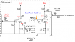
In my forthcoming build I had planned to have an effects loop (Merlin's serial) for using reverb / delay pedals. However, looking at some of the Belton-based pedals out there, it wouldn't be too much of an issue to incorporate the pedal's board internally, inserting it just after the return jack & before the recovery stage grid leak resistor (attached). The goal is simple, usable, post-distortion reverb without the hassle of additonal cables / power supplies etc.
Anyone see an issue with this?
I can use a spare 5V or 6.3V tap to generate a 9V regulated DC supply for the reverb board using a voltage doubler.
Or I could ditch the tube effects loop and do a solid state one instead - saving space...
Anyone see an issue with this?
I can use a spare 5V or 6.3V tap to generate a 9V regulated DC supply for the reverb board using a voltage doubler.
Or I could ditch the tube effects loop and do a solid state one instead - saving space...
Attachments
The only one I can think of is the maximum signal level - I suspect even the cathode of a 12AX7 can put out a bigger signal than most 9V guitar pedals can accept, unless you pad it down.Anyone see an issue with this?
I've never built an FX loop, but if I do, it will almost certainly be solid-state. We're not looking for distortion in the loop electronics, so using a couple of MOSFETs with a little local negative feedback to control gain and reduce distortion below audibility makes sense to me. And that frees up a 12AX7 to use somewhere else, where it really can make a difference to "tone"!
(As an aside, it still frustrates me from time to time, that in the world of guitar we use "tone" where we should be using "timbre". But I guess the misuse is here to stay!
") )
)-Gnobuddy
Thanks - and I'm leaning towards making up a small PCB for a solid-state loop combined with the Belton module.
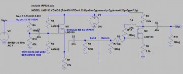
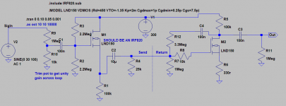
There are so many schematics out there, all seemingly 'the best', for inspiration. A scan of google suggests an IRF820 as a source follower for the send signal, and an LND150 for the recovery.
Attached is my 1st stab, but I'm a bit clueless with solid-state stuff so all input welcome!
I'm assuming a 30V input signal and I am aiming for unity gain across the loop, with a trim pot at the front for adjustment. There would be a send level pot represented by R4. I've no idea if the FETs are biased correctly & I had to use an LND150 for the send as I couldn't get the IRF820 model to work...
I'd tap the return off and follow the Rub-a-dub Deluxe schematic ( http://1776effects.com/wp-content/uploads/2015/03/Rub-a-Dub-Deluxe-BOM.pdf ) for reverb. Thus requiring the 9V and 5V regulators as overhead.
Or if I was really lazy, I could simply put a 9V regulator inside my amp with a panel mount DC jack socket - this could feed an external pedal inserted in the solid-state loop.
With the extra space in my chassis I'd look at putting a 2nd preamp - one input for the October, one input for a JCM800-style. Mixing before the 3rd stage / CF.
So many options!
Attachments
Your proposed biasing scheme on the "send" side should work fine. 
On the receiving side, there are a couple of issues. The first one is that FETs have pretty wide parameter spreads - they're nowhere near as consistent as vacuum tubes. So it's very likely that the actual LND150 you plug into your circuit won't behave quite like the model in LTSpice when it comes to biasing. My experience (mostly with JFETs rather than MOSFETs) is that if you're going with self-bias, you literally have to use a DMM and select the source resistor to match the specific individual FET you happen to be using.
The second issue is the feedback from drain to gate on the receiving side. This type of negative feedback senses and corrects the output voltage by feeding back a current to the input, and is sometimes called a "shunt-shunt" feedback layout ( https://www.electronics-tutorials.ws/systems/feedback-systems.html )
This type of feedback had two characteristics that aren't ideal for this particular application:
1) The amount of negative feedback (and therefore the voltage gain of the FX recovery stage) depends on the output impedance of whatever is plugged into the FX loop. Which means it's unknown and out of your control.
2) Shunt feedback like this lowers the input impedance, which if taken too far, is also not ideal in an FX return.
So I would be tempted to revisit the FX return / recovery stage. I have some thoughts that might be helpful, but work calls at the moment. I will do my best to get back to this thread later today.
-Gnobuddy
...very likely that the actual LND150 you plug into your circuit won't behave quite like the model.... have to use a DMM and select the source resistor....
The series-shunt connection significantly improves the bias stability re: device variation. (As plate falls, grid turns-off, plate rises.... it finds a balance.) Also the signal level is low so bias does not have to be precise.
...the feedback from drain to gate ... lowers the input impedance, which if taken too far, is also not ideal in an FX return.
The FET will give gain a bit over 100. 3.3Meg/100 is 33K. This is not a wrong load; we find loads from 22K to way-high. It will voltage-drive (no NFB) from bass to upper midrange; the highs are generally tuned to taste with loading, a cap, or just ignoring it (the wet path response is a secondary concern).
I'm talking about the LND150 with a 330 ohm source resistor and 100k drain resistor. As I recall from the datasheet, Idss and Vgs(off) for the LND150 vary over something like a 3:1 range; as a result, in this circuit, some LND150s might end up in full saturation, while others might be nearly cut off.The series-shunt connection significantly improves the bias stability re: device variation.
DC gain from source to drain is about 300 times, so a 1 volt change in Vs can cause the drain quiescent voltage to vary by 300 volts...
Personally, I have no confidence that this particular circuit would actually bias up to a usable operating pointk, so I do believe using a DMM and selecting the 330 ohm resistor under test will be necessary to ensure any random LND150 will function in this circuit.
But that's not necessary - we can do much better, with very little additional complexity. Simply bias the gain recovery stage the same way as the FX send buffer stage, using a voltage divider to set the gate to maybe 20 volts or so. Use a roughly 20k source resistor, and you can pretty well guarantee Id will settle at 1 mA, plus or minus a few percent, because the steady 20 V will swamp small FET-to-FET variations in Vgs.
With a 100k drain resistor and 20k source resistor, AC gain is now only 5, but this is easily fixed by paralleling the source resistor with a decoupling cap and series resistor, said resistor being chosen to create the appropriate voltage gain.
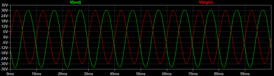
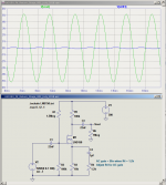
The attached schematic shows what I came up with. Input voltage is 100 mV peak, output 5V peak. The AC gain is set to 50x (i.e. 34 dB), if we believe in the accuracy of the LND150 Spice model, and can be adjusted by varying R4.
The FET biases up to a hair over 1 mA quiescent current, and this will be quite stable because there is about 19 volts nominal at the source, so even a 1-volt variation in Vgs only causes a 5% change in Id.
Okay, you're right, the Zin is acceptable. But what does the 3.3 Meg actually do? If the FX return is fed from a pedal with very low output impedance, the 3.3 M resistor does nothing at all (provides no feedback). If, on the other hand, the stage is fed from an FX pedal that has an unusually high output resistance, the gain of the LND150 recovery stage drops to [3.3M/(output resistance of FX pedal)], which is poorly defined and out of our control.The FET will give gain a bit over 100. 3.3Meg/100 is 33K. This is not a wrong load;
Again, we can do better...simply size the AC-coupled source resistor to set gain, as mentioned in the previous paragraph, and shown in the attached schematic.
The second attached file is the .asc file, you can directly open it in LTSpice if you want to tinker with the circuit.
Danger Will Robinson, Danger! I have not done anything to limit the high-frequency bandwidth of the LND150 - it might not hurt to add appropriate circuitry. A 100 pF cap in parallel with the 100k drain resistor, or better, from drain to ground, should do the trick.
-Gnobuddy
Attachments
Thanks both.
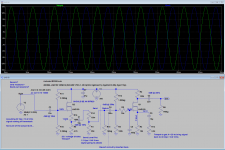
Attached is my latest attempt taking on board those tips and some further trawling through the archives.
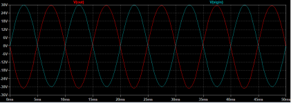
I've used a split cathode resistance to drop the signal (A=0.05) for the send (as well as having an send adjust pot). The recovery is set to A=20. I've tweaked the capacitors values throughout.
As I've no idea what the signal level coming off my tone stack will be I've assumed 30Vpp, and the drop gives 1.3Vpp.
I'm still unsure if I need to add some back to back zeners to ground on the gate of the two Mosfets, and if I need grid resistors and break-out resistors like Merlin would recommend on valves.
What do you think?
I'll also try to get the IRF820 model to work!
Attached is my latest attempt taking on board those tips and some further trawling through the archives.
I've used a split cathode resistance to drop the signal (A=0.05) for the send (as well as having an send adjust pot). The recovery is set to A=20. I've tweaked the capacitors values throughout.
As I've no idea what the signal level coming off my tone stack will be I've assumed 30Vpp, and the drop gives 1.3Vpp.
I'm still unsure if I need to add some back to back zeners to ground on the gate of the two Mosfets, and if I need grid resistors and break-out resistors like Merlin would recommend on valves.
What do you think?
I'll also try to get the IRF820 model to work!
Attachments
Some MOSFETs have built-in Zener protection, but from the datasheet, I don't think the LND150 is among them. So I think it's wise to include external Zeners - I use two series, back-to-back, 12 volt Zener diodes, with a "gate stopper" to limit overload current through those Zeners if the input does get heavily overdriven.I'm still unsure if I need to add some back to back zeners to ground on the gate of the two Mosfets, and if I need grid resistors and break-out resistors like Merlin would recommend on valves.
I have a tiny bit of anecdotal evidence to offer: I've read at least a couple of online tales about people using LND150s to create "source-o-dyne" phase splitters, and having the MOSFETs die after a short time. In those cases, no external Zeners were used. Meantime, I have an LND150 source-o-dyne PI in a guitar amp I built a couple of years ago, and it has given me no problems at all. There is a gate stopper (47k, I think, though I've tried up to 1 Meg there), and a pair of series back-to-back 12 V Zeners.
On the build-out resistors, my thought is, why not include them? They definitely won't do any harm, and might do some good, so why not?
Incidentally, why not use an LND150 for both send and receive stages? I don't think you need the additional current capability of the larger IRF MOSFET, and you don't have to worry about the exposed metal tab on a TO-220 package sitting at full B+ voltage to shock the unwary...
One of the good things about this method of biasing FETs using a fixed DC gate voltage chosen to be >> Vgs, is that the circuit has very little sensitivity to variations in FET parameters - which you've confirmed by finding that it makes almost no difference what MOSFET you throw into the circuit!
-Gnobuddy
Thanks Gnobuddy,
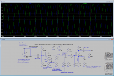
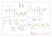
Attached is an updated schematic for the effects loop, the reverb circuit and an attempt at the power supply for it all.
How does it look?
The more I dig the more I find other, similar, approaches to a loop circuit using the LND150. Differing approaches to attenuation and setting the recovery gain. Differing values of coupling capacitors etc. It seems people are happy with ~3dB roll-off at around 100Hz.
So this schematic is probably a bit over complicated compared to others but if I avoid any issues biasing the LDN150, have control of the gain across the loop and have a flat-ish frequency response, then great.
T
Attachments
Looks pretty good to me, though you never know till you build and try it!How does it look?
I had a possibly useful thought - if you break R15 into two resistors, say 1Meg + 470k, and solder a small cap from the junction to ground, you can filter away a lot of noise from the B+ rail before it gets to the input (gate) of the recovery MOSFET. Even a small 100nF cap will provide at least 20 dB of hum filtering at 60 Hz, and more at higher frequencies. Something like 1uF would really clean up any B+ noise, and may make the recovery stage quieter and more hum-free.
With this circuit, the thing I'm least sure of is the proper send level and/or recovery gain. In my experience, even two small audio mixers often disagree about what they expect for "line level", and then there are the additional complexities of "instrument level", whatever that is in the manufacturers mind.
One would think at least guitars and guitar-specific FX pedals would get along, but I have some guitars and guitar pedals that are not a happy fit - like my Ibanez AS-73 semi-hollow guitar, which is capable of clipping my Joyo compressor and making it sound like a bad fuzz-box!
I tend to err on the side of overkill, so if I was putting together this FX loop for my amp, I might consider an adjustable pad (maybe -10 dB) on the send side, as well as a variable send level pot. And maybe the same two things on the recovery side as well, i.e. a switchable pad and variable recovery gain. At which point the FX loop is probably more complicated than the entire preamp in a Fender 5E3!
I've certainly seen some very simple FX loop designs in DIY designs - one which makes me shudder simply uses a 1 Meg volume pot to adjust the send level, and introduces up to 250k output impedance at the same time! But the guy who built that amp seems quite happy with it.
-Gnobuddy
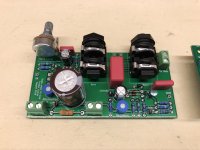
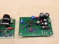
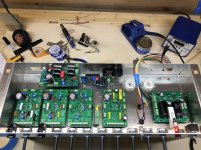
So I got the boards manufactured and have now populated them. Next is getting the amp built which they'll go in to!
Will report back if / when it works.
I'll have a few PCBs spare should anyone want one.
Will report back if / when it works.
I'll have a few PCBs spare should anyone want one.
Attachments
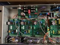
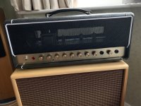
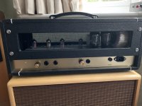
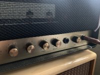
Thanks - below is what they are going in to.
More details here: AX84.com - The Cooperative Tube Guitar Amp Project
More details here: AX84.com - The Cooperative Tube Guitar Amp Project
Attachments
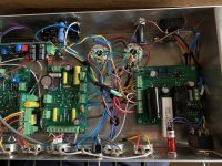
Very nice soldering and build! You have good hands!So I got the boards manufactured and have now populated them.
-Gnobuddy
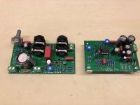
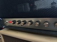
A quick update to say this design / PCBs are working well in my new build. I used the Belton with a 'medium' length of reverb and it sounds pretty good so far. I've put up some details of the build here,
Also, the whole genesis of this was here: AX84.com - The Cooperative Tube Guitar Amp Project
I've a few spare PCBs if anyone wants to try them out.
Also, the whole genesis of this was here: AX84.com - The Cooperative Tube Guitar Amp Project
I've a few spare PCBs if anyone wants to try them out.
- Status
- This old topic is closed. If you want to reopen this topic, contact a moderator using the "Report Post" button.
- Home
- Live Sound
- Instruments and Amps
- Adding Belton reverb module / pedal to amp