This amp has a blown output transistor. It is a TO-3 package. It is marked "RCA" and "101568".
I have searched the NTE equivalent database, as well as the alltransistors.com database, no luck. From the markings, the "68" could also be a G8, a 6B, or a GB.
Can I throw a pair of 3055's in here and rebias? I don't have the original schematic, either.
Thanks everyone.
I have searched the NTE equivalent database, as well as the alltransistors.com database, no luck. From the markings, the "68" could also be a G8, a 6B, or a GB.
Can I throw a pair of 3055's in here and rebias? I don't have the original schematic, either.
Thanks everyone.
CALL Fender on the phone and ask if they have documents on this ancient warrior.
101568 would most likely just be a Fender part number. So it is not a type of transistor.
Without seeing the schematic or having the live unit before me, it is impossible to say if 2N3055 would be good there. What are the supply voltages? How many transistors in parallel for what power output?
101568 would most likely just be a Fender part number. So it is not a type of transistor.
Without seeing the schematic or having the live unit before me, it is impossible to say if 2N3055 would be good there. What are the supply voltages? How many transistors in parallel for what power output?
Replace both power transistors.
Use MJ15022 which has become the "universal" NPN TO3 power transistor in old Musical Instruments amplifiers, instead of "selected 2N3055" and whatnot.
No current 2N3055 will fit there.
You *might* have to replace drivers too and check for low value emitter resistors to still be alive, many times they work as fuses and open.
Attachments
Holy Mackerel,
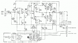
I received an email immediately after pressing the post button on that last reply. Brett from Fender did another quick search and found the full schematic. I am posting it for everyone, and it does show the actual transistor numbers for the OT's. Thanks guys, Great Day!
I received an email immediately after pressing the post button on that last reply. Brett from Fender did another quick search and found the full schematic. I am posting it for everyone, and it does show the actual transistor numbers for the OT's. Thanks guys, Great Day!
Attachments
I note the 1568 on the drawing, which brings me back to the part number. Fender uses 10 digit numbers now, but 45-50 years ago not so much. Also, many times part numbers are abbreviated by leaving off leading or trailing zeros. I am glad they came through for you.
I wonder if they used this amp chassis in any of the Rhodes models. I will look. The drawing style is reminiscent of the Rhodes stuff.
I wonder if they used this amp chassis in any of the Rhodes models. I will look. The drawing style is reminiscent of the Rhodes stuff.
2N3772s aren't that hard to find - and can be replaced with 3773 or any NPN MJ150xx. The 2N3054 drivers would be more problematic. Try finding any TO-66 these days. You could use TIP41C if you retrofit for TO-220. Not impossible, but not something everyone is willing to do. Often considered a "hack job".
Yes.
TO220 were *designed* to replace TO66 metallics.
You have to bend legs down to fit through old holes, and, of course, use a single screw for mounting but dimensions match.
Same with TO3P : early ones were oval/egg shaped, to fit in heatsinks molded for metallics, then evolved into TO218 when new designs were made specially around them, and finally into simpler to mount TO247.
Often new Technologies have to copy old designs, not for Technical reasons but to help old users switch without redesigning everything from the ground up.
EDIT: and instead of hunting for obsolete 2N377* , or even MJ15015, go straight to MJ15022 which supersedes them all , is in current production, and to boot costs all of 4 bucks.
And I learnt that from Enzo")
TO220 were *designed* to replace TO66 metallics.
You have to bend legs down to fit through old holes, and, of course, use a single screw for mounting but dimensions match.
Same with TO3P : early ones were oval/egg shaped, to fit in heatsinks molded for metallics, then evolved into TO218 when new designs were made specially around them, and finally into simpler to mount TO247.
Often new Technologies have to copy old designs, not for Technical reasons but to help old users switch without redesigning everything from the ground up.
EDIT: and instead of hunting for obsolete 2N377* , or even MJ15015, go straight to MJ15022 which supersedes them all , is in current production, and to boot costs all of 4 bucks.
And I learnt that from Enzo
That's probably why 3772s were used instead of 3055's. The old hometaxial 377x would tolerate a shorted output on these relatively low voltages. 3055 probably won't. I'm betting 15024's or 3773's would take a short just fine. That old topology is pretty robust with wide-SOA silicon NPNs.
EDIT: and instead of hunting for obsolete 2N377* , or even MJ15015, go straight to MJ15022 which supersedes them all , is in current production, and to boot costs all of 4 bucks.
And I learnt that from Enzo
And if another suitable type happened to be on hand it would effectively be free instead of costing $4 plus freight and tax. if you're going to buy new it only makes sense to buy a 15024 or 21194. But if you've got a bin full of 3773's or 15003s you could put them in and call it good without waiting for a Mouser order to come in. What I would stick in would be a pair of 2N6258's. Got a dozen or so pulled from working equipment and cost nothing. And a very close match to the original RCA 3772.
Thanks everyone. What's the scoop on rebiasing after I pick a set of output devices that match the design specs? I chose 2n3772's, got a good deal on four of them and now they are here.
This isn't the first time I've encountered an output section repair with no schematic, or with a schematic that does not have biasing information included. Could someone walk me through the steps to rebias a 2 pot design like the fender, or a 4 pot design like this Nikko STA-5010?
This isn't the first time I've encountered an output section repair with no schematic, or with a schematic that does not have biasing information included. Could someone walk me through the steps to rebias a 2 pot design like the fender, or a 4 pot design like this Nikko STA-5010?
Attachments
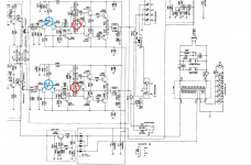
The Fender: you want to get 30-60mV across each emitter resistor (here two 0.2r in series), AND you want the output DC to be very small (few Volts no-load, <1V with speaker). But the two pots interact. I would start both dead-short. Trim one to get just a few mV across the 0.4r. Then trim the other the same. Increase to a dozen mV, both. Now check the output DC and trim one pot so the DC is small. At that point I would try to play. If it sounds good, call it done. Over-biasing might be safe here (the diodes put a limit on the bias) but if not, you smoke the whole output stage.
The Nikko is far simpler, and should be clear?
The Nikko is far simpler, and should be clear?
I now realize "how small" the current requirements are for most output transistors in order to get them into the linear region of operation.
(Question 1)
I'd like a little further understanding of basic biasing theory.
If a single TO-3 transistor "turns on" correctly between 30 and 60mA, is there a way to "see" that I have set the bias at the correct amount? Can I use a scope on one leg of the push-pull and see a "non-linear/linear" point being crossed as I adjust the value of the trimpot? Do some amp builders use distortion analyzers, etc to determine an exact bias point?
(Question 2)
Is there a special name for the XS in the Nikko schematic that sets the bias for the whole output circuit? How exactly does this XS (Q659, Q660) perform its function?
(Question 3)
If the trimpots were not in the Fender circuit, would the base bias voltage for the driver XS be determined by the Vdrop of the stacked diodes? I'm digging deeper into what PRR has said about the diodes and their role in the biasing. Similarly, if the stacked diodes were not in the schematic, would the amplifier be more likely to go up in smoke if a trimpot were to fail??
(Question 4)
Why didn't the designers use PNP devices in the bottom half of the Fender schematic? I don't fully understand the Fender schematic, unless... The ISXF doesn't actually split phase here, but does deliver (2) identical signals... and all of the output devices are acting as current drivers. The ISXF could produce all of the extra Vgain that an output stage would want.
(Question 5)
The Nikko amp. After adjusting the bias, I should then adjust the balance pot at the LTP with the help of a scope, while the output is driven to the edge of clipping?
(Question 6)
How important is the Beta value of each preceding signal transistor before the Output XS in the Nikko design?
Thanks. I'm having fun.
Question4 - because the 2N6609 hadn't been invented yet. Decent PNP's were unobtainium when the amp was new. The ones you could get were junk, cost $12 a piece, or germanium. Pick your poison.
The output stage is a simple common emitter and has voltage gain. One transistor handles the positive half cycle and the other the negative. They are driven out of phase. The signal goes across the base-emitter (plus some degeneration, which is also used for bias stability) and the output is taken off the collector to an AC ground. The power supply is connected in a different place on the top half compared to the bottom, but for purposes of AC analysis that does not matter. It only matters where the signal goes in and where it comes out when it comes to classifying a stage as to common emitter or whatever, and for the purposes of calculating gain.
The output stage is a simple common emitter and has voltage gain. One transistor handles the positive half cycle and the other the negative. They are driven out of phase. The signal goes across the base-emitter (plus some degeneration, which is also used for bias stability) and the output is taken off the collector to an AC ground. The power supply is connected in a different place on the top half compared to the bottom, but for purposes of AC analysis that does not matter. It only matters where the signal goes in and where it comes out when it comes to classifying a stage as to common emitter or whatever, and for the purposes of calculating gain.
....The output stage is a simple common emitter and has voltage gain...
Thank you thank you! I discussed such an amp in another place with a guy who should know better, but said it was a "mix of CE and CC".
Complete from scratch theory of smoothing an AB amp is long and tedious. Since this amp is designed, we go with the emitter resistors we find. We want enough current so the Emitter Impedance (hIE), seen looking into the emitter, is similar to the emitter resistor. hIE is 30 Ohms at 1mA, so 1 Ohm at 30mA, and near 0.4r at 75mA. So for very-very small signals, the output looks like (0.4+0.4)||(0.04+0.4) or 0.4 Ohms. And for very large signals, say 1 Amp, hIE falls to 0.03r on one side and near infinity on the other, giving 0.43r, about the same as at idle.
However the impedances at the base also matter.
And full understanding came long after tranny amps were widespread. You may find very different procedures in old manuals (if you can find the old manuals...)
However a STAGE amp is almost never played so soft that a trace of crossover distortion will get you thrown out of the club. And in a very crude amp like this, I would err on the side of too-cool.
The Nekko is a very different design and deserves its own thread (and maybe not in Instrument Amps).
That is all very interesting. I understand that the bottom transistors have their collector tied to the AC signal output... where is the signal being taken from on the top transistors?
* I can't find any .2r 10W resistors in the chassis or on the circuit board. There is one 10W resistor, a 100r, and it is not on the schematic. I believe it has been placed where the bottom .4r is supposed to go, as it is tied to the emitter and the NEG terminal of the leftmost Filter Capacitor, as seen in the schematic.
* I can't find any .2r 10W resistors in the chassis or on the circuit board. There is one 10W resistor, a 100r, and it is not on the schematic. I believe it has been placed where the bottom .4r is supposed to go, as it is tied to the emitter and the NEG terminal of the leftmost Filter Capacitor, as seen in the schematic.
From the top transistors the signal still comes out of the collector. It goes THROUGH the power supply (which is an AC short), up thru the minus terminal of the speaker, thru the output cap, to the common emitter terminal. Going backwards thru the speaker provides the phase reversal needed because the bases are driven out of phase. The "common " terminal is the one which is common to both the input and output, and does not have to be global ground. It's like one half of the amp has the power supply "inside out". Crazy, but it works.
It is really very similar to Elvee's "Circlophone". His has a unique differential drive and bias servo, but the operation of the output stage is essentially the same. With CFP's instead of darlingtons, and a polarity reversal. These amps were often made with germanium PNP's using a driver transformer like this one. The use of the split phase driver transformer was preferred in the olden days because of very slow output transistors. They put the transistor vbe into hard reverse bias during the off half cycle, enhancing the breakdown voltage and speeding up the turn off. Neither happens with a standard complementary push pull.
It is really very similar to Elvee's "Circlophone". His has a unique differential drive and bias servo, but the operation of the output stage is essentially the same. With CFP's instead of darlingtons, and a polarity reversal. These amps were often made with germanium PNP's using a driver transformer like this one. The use of the split phase driver transformer was preferred in the olden days because of very slow output transistors. They put the transistor vbe into hard reverse bias during the off half cycle, enhancing the breakdown voltage and speeding up the turn off. Neither happens with a standard complementary push pull.
- Status
- This old topic is closed. If you want to reopen this topic, contact a moderator using the "Report Post" button.
- Home
- Live Sound
- Instruments and Amps
- Fender CFA7001 PA Amp - Looking for equiv. RCA output transistors